
The information in this document is believed to be reliable, though no responsibility is assumed for inaccuracies. The San Diego State Astronomy Department reserves the right to make changes to the items described herein to improve reliability, function or design. Neither San Diego State University, San Diego State University Foundation, nor any of their employees, including the people named immediately below, assume any liability for damages, either direct or incidental, that may arise out of the application or use of any of its products or circuits, particularly with regard to damage that may occur in the operation of delicate and costly charge coupled devices (CCDs) or infrared arrays.
For further information about optical CCD camera electronics and systems contact -
Bob LeachFor further information about infrared camera electronics and systems contact -
Frank LowThe Astronomy Department at San Diego State University has developed a set of versatile camera electronics designed to control a wide variety of optical and infrared imaging arrays. Originally designed for operating CCDs in a slow scanned readout mode, the electronics have been broadened to operate optical CCDs in a fast readout mode of up to one microsec per pixel that efficiently supports many simultaneous readouts. In conjunction with Infrared Laboratories, Inc. of Tucson AZ two new boards have been developed to operate infrared arrays in this fast readout mode that are suitable for operating HgCdTe, InSb and other infrared arrays. The large dynamic range of CCDs and infrared arrays is maintained through the use of low noise techniques and 16-bit A/D converters. These controllers are usable for a variety of both optical and infrared image sensors and have been operated by a number of groups worldwide. There are presently thirty institutions worldwide using these controllers for a wide variety of sensors, including Tek 1024 and 2048 square CCDs, Loral 2048 square and 2048 x 4096 CCDs, and infrared NICMOS III arrays. The operation of CCD and infrared arrays are so similar that the controller electronics will be described for both cases interchangeably except where differences arise, and the generic term 'array' will refer to both CCD and infrared array imaging detectors.
The camera electronics described here is targeted to operate one or more CCD or infrared arrays, each containing one or more readout circuits, at readout times as fast as one microsec per pixel, or one megapixel per second. From one to about 16 readouts can be operated efficiently with one set of camera electronics. The arrays will normally be cooled thermoelectrically or cryogenically to reduce thermal dark current generation. Considerable flexibility has been built into the design to allow operation of a variable number of readouts, as well as operation of a wide variety of both optical and infrared arrays in such modes as staring, drift scan, shuttered and frame transfer. They can be programmed by the user to meet a wide variety of applications, and several programs are supplied to handle simple configurations and to provide the user with a starting point in customizing their systems.
This manual describes in detail the electronics and software elements of the camera system , including hardware and software preparation, system installation, theory of operation, and performance. To improve the utility of this document, its chapters are updated from time to time, and the most recent revision dates of each chapter are written at the bottom of each page. Backup copies are kept in an archival directory as significant changes are made and copies are accessible on the Web.
Files are available via ftp on suicide.sdsu.edu, username anonymous, password 'your e-mail address', directory pub. The revision number of the software and circuit boards that is described are listed at the top of each chapter.
Below are listed the major components available, with a short description of each -
This section describes the major system components in moderate detail. The electronics board are described first, followed by the mechanical, power supply, dewar and host computer software components. Detailed chapters about the major components follows.
The heart of the digital timing board is the Motorola DSP56002, a monolithic, integer digital signal processor with a 24-bit data word. It has a 16-bit address space, a fast ALU, extensive on-chip peripheral support and a Reduced Instruction Set Computer (RISC) architecture that executes most instructions in one clock cycle of 40 nanosec. The DSP has separate address spaces for on-chip program and data memory, a synchronous serial interface, boot logic and a simple interface to an external data bus. It functions as a timing generator by writing 24-bit data words from memory to its external bus every 40 nanosec, which are decoded by timing board circuitry to enable various hardware functions. Eight of the 24 bits enable a delay function that halts processor operation for intervals ranging from 100 nanosec to 20.4 microsec in 20 nanosec increments to implement programmable delay timing. The remaining 16 bits are written to the backplane for decoding by the clock driver and video processor boards. Synchronous serial communication provided by the DSP is used to communicate with the utility board and to send digital voltage data to all the DACs in the system.
On power-up or reset the DSP program is read in from a boot ROM, which is a single byte-wide socketed device for easy re-programming external to the controller. Programming is done on a cross compiler supplied by Motorola in native DSP56002 assembly language. The supplied DSP program consists of initialization code to configure the DSP in the desired mode, a command processor, testing and diagnostic routines, routines to read from and write to internal DSP and boot ROM memory, tables containing readout parameters and timing waveforms, and array readout code. Modifications to the code can be done either by re-programming the ROM or by modifying the DSP contents over the fiber optic link from the host computer. Thirty two kilowords of external memory are provided on the board for no wait state access by the DSP to supplement its internal memory. A fast fiber optic data link processes commands, generates replies and writes image data to and from the host computer, operating at 4 MHz for receiving incoming commands and 50 MHz for transmitting replies and image data, providing a maximum image data rate of 2.5 megapixels per second, or 400 nanosec per pixel. This will support five readouts at the nominal processing time of two microsec per pixel.
The parallel cable version of the timing board is similar to the fiber optic version, but instead has support for a 16-bit parallel image data link that transmits over commercially available SCSI-3 cable to a host computer interface card for PCI buses designed by Spectral Instruments of Tucson, AZ. The cable will support very high data rates and is presently implemented at 6 Megapixels per second. Command and reply communication is implemented over the DSPs asynchronous serial interface with RS-422 drivers operating over the same parallel data cable.
A DC coupled preamplifier with an input offset adjustment is followed by a stage with four switchable gains. A polarity reversing set of amplifiers drives a resettable integrator to implement a dual slope integrator. A fast sample/hold operates at x2 gain to drive the A/D converter and provide a second stage of offset adjustment. Two complete video processors are provided on each board.
Potentiometers are not used anywhere in the controller, as all adjustable voltages are set digitally by the DSP. The analog board is implemented on a six-layer printed circuit card with careful isolation between digital grounds, the noisy analog and digital ground surrounding the clock drivers and logic circuitry, and the quiet analog grounds in the video processor. Ground planes are placed liberally throughout the circuit, and a careful physical placement of components isolates these circuits as well.
A preamplifier operates at x5 gain and contains an input offset circuit to remove the bias of the incoming array signal. A unity gain inverting stage is needed to present the correct polarity to the A/D converter, followed by a sample/hold switch and a x2 gain stage to allow the S/H switch to operate over the range of 0 to +5 volts and the A/D over the range of 0 to +10 volts.
The clock driver board supplies a total of 24 clocks for driving CCD or IR arrays over a range of +10 to -10 volts. The clock voltages are set by 12-bit DACs with a resolution of about 10 millivolts. Two DAC output voltages are used by each clock driver circuit, with a fast analog switch selecting one of the two DAC voltages for amplification by a fast op amp. Low noise (less than 10 nanovolts per root Hertz) and fast (40 nanosec switching times for a 20 volts swing) circuit techniques are used. Protection against overvoltages that could damage sensor arrays are provided by zener diodes on the voltage reference circuit, by user-configurable blocks of zener diodes on each clock driver output circuit and by analog switches placed at the output of each clock driver circuit that is controlled by the power monitor of the power control board and by software control from the timing board.
The utility board provides a miscellany of support functions that are not directly involved with readout of the arrays. These include, but are not limited to, exposure timing, array temperature control, and system voltage and temperature monitoring. Based around a DSP56001, it is programmed to support these functions, and can be programmed by the user to support other functions (such as an additional temperature controller, dewar level and ID, shutter status, LED driving for status, switch monitoring for direct system control without a host computer) by programming the use of a number of uncommitted I/O pins. Communication with the timing board can be either through the asynchronous serial port of the timing board's DSP, through a 9-pin RS-232 connector on the utility board, or through two asynchronous serial lines on the backplane.
The power control board conditions the DC power to protect the array from overvoltage transients. The board passes three analog voltages (high voltage, nominally +32V, and low voltages, nominally +/- 15V) from the power supplies to the backplane in a controlled manner so that short high voltage spikes are not passed on to the analog board. The board plugs into the back of the backplane, is parallel to it, and is six slots wide. It allows the utility board to turn on switches only after the digital supply has stabilized, all DSPs have had their software loaded and the DACs on the analog boards have all been set to their proper values. On command from the utility board the power control board slowly turns on the +/-15V supplies to the system backplane following a linear ramp of about 40 millisecs duration, after which the high voltage is switched on after the utility board signal. A bank of comparators examines the three analog supplies and the ave. digital supply to prevent any of the analog supplies from being switched on to the system backplane if any of them are out of range, and turning off all analog supplies in the event of a power supply failure after the power has been turned on. A power-on reset circuit examines the digital supply and resets the utility board if is is not within range.
The VME interface board provides a communication path between the fiber optic link on the timing board and the host computer. It sends commands from the host computer to the timing board following the 24-bit protocol of the serial link, and accepts image data from the timing board and writes them to VME memory using an on-board DMA (Direct Memory Access) controller. Image size is only limited by the 32-bit addressing range of the VMEbus, as entire images can be written to VMEbus memory without intervention from the host processor. This allows non real-time operating system such as UNIX to be used in the host computer, and permits concurrent operation of the host computer even during image readout. Exposures are initiated by the host computer, timed by the utility board, then placed into memory by the interface board, after which the interface board signals to the host processor that the image is available in memory so it can be processed, displayed and stored by the host computer.
The interface board utilizes a DSP56001 processor for housekeeping and DMA address generation. A local buffer memory (32k x 24 bits) stores incoming image data to avoid lost data if the VMEbus is unavailable for short periods. Interrupts can be generated by the interface board, and VMEbus memory can be written to or read from under control of the on-board DSP. The host computer communicates with the interface board by writing to a single memory mapped address, and is denied direct access to the on-board buffer memory.
The Sbus interface board that communicates over the fiber optic data link between the timing board and a host computer containing SBus slots, which are commonly found on workstations manufactured by Sun Microsystems. The board serves the same function as the VMEbus interface described in earlier, but has the advantage of plugging directly into Sun workstations. This may be of interest to users of Sun workstations since an intermediate VMEbus chassis, memory and communications link are no longer necessary. The interface board contains a DMA (direct memory access) controller with 24-bit word and address counters that writes image and reply data directly to Sun system memory without processor intervention, enabling large images to be read out without burdening the host processor. Lacking a DSP, it does not perform any processing such as de-interlacing or two's complement calculation on the incoming images.
Spectral Instruments, Inc. of Tucson, AZ.
The backplane is simply implemented as a VMEbus J1/P1 backplane whose pins and timing have been completely redefined for this application. 96-pin DIN connectors provide a plentiful number of reliable pins, while the multilayer backplane provides good power distribution and noise suppression. DC power is distributed to the boards through the backplane, using the +5 connection for +5 volts, whereas the +/- 12 volt connection is powered with +/- 15 volt supply that is then down-regulated to +/- 12 volts on each analog board. The high voltage supply, nominally +36 volts, that is required for operating the drain of the CCD on-chip amplifier is brought onto the analog boards separately, to insure low noise operation, and is heavily filtered as well. The boards are all of the standard VME 3U width, that is, roughly four inches wide, but longer than the VME standard by about 50%. The number of VMEbus boards used in a particular installation is determined by the number of analog readout boards that are required; up to 21 connector VME backplanes are available, allowing 19 readouts if a timing and utility board are installed. It is expected in typical installations that the backplane and controller boards will be mounted as close as practical to the array, which is typically on the side of the cryogenic dewar containing the arrays. Robust grounding of the analog boards at the array connector end is required for low noise operation in multiple readout configurations.
The backplane supports full 24-bit data words on both reading and writing. While the analog readout board reads 16 of these bits, it writes 16 bits containing image data and an 8-bit identification tag that is equal to the jumpering of the address selection jumper block. our address lines, A00-A03, are carried on the backplane in order to address the A/D converter when transferring pixel image data to the DSP. This makes the backplane a D24:A04 system. It is not a bus in the normal sense since only the timing board can be a master, and no bus arbitration circuitry is needed. A complement of 21 timing signals generated by the timing board are also carried over the backplane, while only seven of these are currently used by the analog board. These additional signals could be used to operate such devices as a programmable array temperature controller, a shutter, diagnostic hardware, filter wheels and so on. Two interrupt input lines to the DSP are also available on the backplane, which can be used to implement a hardware timing circuit for overall exposure timing that would be independent of the host computer.
The controller boards are housed in a rugged box that is attached to the side of a cryogenic dewar. It is mounted to the dewar on four standoff spacers, and contains a hole in the baseplate for passing through a 61-pin hermetically sealed circular connector attached to the dewar. Short wires run from this connector to the analog and utility boards, and are totally enclosed by the housing for electrical isolation from potential external sources of interference. The housing contains a six slot VME backplane that accommodates a timing board, a utility board, a clock driver board and and three video processor boards for implementing six readouts. It also has a power control board, and internally mounted fans. Built of aluminum, it has a skeleton to which removable panels are attached with screws for easy access to the controller boards for diagnostic probing. Six panels, all except the bottom plate that attaches to the dewar, can be removed while the controller is operational. The box is sealed from the outside so cooling occurs by circulating air inside the box through the boards, relying on heat conduction to the box. This is done to minimize dust and dirt contamination of the controller boards and to allow the boards keep their internally generated heat when operated in cold climates. The outside housing dimensions are (inches) 13.25 L x 6.75 H x 5.50 W, or (cm) 33.30 L x 16.20 H x 14.0 W.
The standard dewar implemented by SDSU is a model ND-5 nitrogen dewar purchased from Infrared Labs with additions for mounting the CCD, wiring to it and controlling its temperature. Dewars for infrared arrays should be obtained directly from Infrared Labs. Liquid nitrogen tank capacities are available from 1.5 to 3 liters, with the smaller capacity chosen for operating smaller CCD for less than 24 hour hold times, and the larger capacity chosen for greater than 24 hour hold times with 2048 square CCDs. The dewar has an 8-inch diameter front plate containing an AR-coated quartz window in front of a working volume that is six inches in diameter and three inches deep where the CCD is placed. The CCD is placed in a socket that is attached to a glass epoxy support structure that attaches to a clamp ring on the inside of the dewar wall, allowing focal distance, tilt and rotation adjustments with the aid of an alignment jig. Cooling is transferred from the nitrogen cold plate to the CCD with a cold strap that is trimmed to bring the CCD close to the desired temperature and then a small resistive heater actively brings it to the desired temperature under control by the utility board with a small forward biased diode acting as a temperature sensor. A calibrated temperature sensor gives absolute calibration of the CCD temperature to one degree Celsius.
A user interface program is available that executes in the Solaris operating system developed by Sun Microsystems. It operates with either the VMEbus or SBus interface board. In VMEbus systems the CPU chip set is either resident on a VMEbus board that resides in the same backplane as the interface board, or resides in a workstation that connects to a VMEbus backplane over a host adapter or other communications link. The program, named generically "ccdtool", executes on the Sun to acquire images and manage the controller. It is a windowing program written in C with the Xview graphical tools conforming to the OpenLook graphical user interface. It sets up the three controller DSPs with either download or on-board application programs, sets user parameters, issues exposure sequence commands, allows individual manual commands to be issued and writes images to disk in the FITS format. IRAF is used for image display and analysis, reading the images from disk.
A list of salient performance parameters is presented below to give the user some orientation. The meaning of some of the terms may not be apparent, but hopefully some of this will get cleared up in the remaining sections of this manual.
Form Factors:
Power Dissipation
They are controlled by 12-bit DACs, and can be set to within about 10 millivolts. Their long term voltage stability is about 5 millivolts, and their noise is less than one microvolt rms if connected to the input of the video processor board.
Six programmable DC bias supplies on the infrared video processing board provide the following voltage ranges: Six at either 0 to +5 V, 0 to -5V or -5V to +5V, jumper selectable
They can be used for controlling NICMOS arrays (positive voltages) or InSb arrays (negative voltages). They are controlled by 12-bit DACs, and can be set to within about 3 millivolts. Their long term voltage stability is about 2 millivolts, and their noise is less than one microvolt rms if connected to the input of the video processor board.
| Pin # | ROW a | ROW b | ROW c |
| 1 | SS14 | UTL-E-RXD | SS15 |
| 2 | SS12 | UTL-E-TXD | SS13 |
| 3 | SS10 | TIM-A-CDAC | SS11 |
| 4 | SS08 | UTLRST | SS09 |
| 5 | SS06 | *USER | SS07 |
| 6 | SS04 | *USER | SS05 |
| 7 | SS02 | *USER | SS03 |
| 8 | SS00 | *USER | SS01 |
| 9 | GND | *USER | GND |
| 10 | SCLK | *HVEN | AD00 |
| 11 | GND | *USER | AD01 |
| 12 | BUS-CLK | TIM-A-SCK | AD02 |
| 13 | TIM-D-AUX | TIM-A-STD | AD03 |
| 14 | TIM-ADA0 | TIM-ADA1 | AD04 |
| 15 | GND | TIM-ADA2 | AD05 |
| 16 | TIM-ADA3 | TIM-ADA4 | AD06 |
| 17 | GND | TIM-ADSTR | AD07 |
| 18 | TIM-U-WDT | UTL-T-TXD | AD08 |
| 19 | GND | UTL-T-RXD | AD09 |
| 20 | EXT-U-IRQ | GND | AD10 |
| 21 | *LVEN | TIM-U-SCK | AD11 |
| 22 | *PWRST | TIM-U-STD | AD12 |
| 23 | UTL-T-SCK | GND | AD13 |
| 24 | UTL-T-STD | UTL-T-IRQ | AD14 |
| 25 | STATUS0 | EXT-T-IRQ | AD15 |
| 26 | STATUS1 | PWROK | AD16 |
| 27 | STATUS2 | TIM-A-WRSS | AD17 |
| 28 | STATUS3 | TIM-A-ENCK | |
| 29 | TIM-V-AUX1 | LVEN | TIM-U-RST |
| 30 | TIM-LATCH0 | EXT-T-RST | |
| 31 | -16V | +32V | +16V |
| 32 | +5 VDC | +5 VDC | +5 VDC |
* The VME backplane does not bus these signals to all slots.
AD00 -> AD17 Analog-to-Digital converter data. Least significant bit is AD00.
BUS-CLK System clock generated by the timing board for use by other boards.
EXT-T-IRQ Generated by an external source to request a timing board interrupt on IRQB*.
EXT-T-RST External signal to reset the timing board.
EXT-U-IRQ External signal to request interrupt service from the utility board.
HVEN Generated by the utility board to turn on the power control board's high voltage switches.
LVEN Generated by the utility board to turn on the power control board's low voltage switches.
PWROK Generated by the power control board to signal that the power supply voltages are within limits.
PWRST Reset the power control board, and turn off the low and high voltages.
SCLK Serial clock used for asynchronous serial interface in synchronous mode.
SS00 -> SS15 Switch state bits generated by the timing board to control clock driver and video processor analog switches. Bits 0-11 are used for switch states, and bits 12-15 are used for board select.
STATUS0 -> STATUS3 Four programmable status lines running from the timing board DSP general purpose I/O pins to the backplane for general use.
TIM-ADA0 -> Address bits generated by the timing board to select the A/D converter to be read. A total of 32 A/Ds can be read.
TIM-ADSTR Address strobe signal generated by the timing board to cause A/D values to be written to the lines AD0-AD17 by the video board.
TIM-A-SCK Synchronous serial clock from the timing board to analog boards.
TIM-A-STD Synchronous serial data from the timing board to analog boards.
TIM-A-CDAC Clear all the digital contents of the analog board DACs.
TIM-A-ENCK Enable the outputs of all the clock drivers and DC bias supplies on the analog boards.
TIM-A-WRSS The switch states SS0-15 are valid when this signal goes high.
TIM-D-AUX Timing to clock driver board uncommitted communication line.
TIM-LATCH0 Uncommitted latched signal output from the timing board.
TIM-U-RST Generated by the timing board to reset the utility board.
TIM-U-SCK Timing to utility board synchronous clock.
TIM-U-STD Timing to utility board synchronous data.
TIM-U-WDT Generated by the timing board to signal to the utility board watchdog circuit that the timing board is alive.
TIM-V-AUX1 Timing to video processor board uncommitted line.
UTL-E-RXD Utility board to external asynchronous receive data.
UTL-E-TXD Utility board to external asynchronous transmit data.
UTLRST Reset the utility board.
UTL-T-IRQ Generated by the utility board to request a timing board interrupt.
UTL-T-RXD Utility to timing board asynchronous serial received data.
UTL-T-TXD Utility to timing board asynchronous serial transmitted data.
UTL-T-SCK Utility to timing board synchronous clock.
UTL-T-STD Utility to timing board synchronous transmitted data.
Resets, interrupts, and general system support -
EXT-T-IRQ	EXT-T-RST		EXT-U-IRQ		UTLRST
TIM-U-RST	UTL-T-IRQ		BUS-CLK			TIM-U-WDT
STATUS0 ->  STATUS3
Serial communication -
TIM-U-SCK	TIM-U-STD		UTL-T-SCK		UTL-T-STD
TIM-A-SCK	TIM-A-STD		SCLK
UTL-T-RXD	UTL-T-TXD		UTL-E-RXD		UTL-E-TXD
Power control board functions -
LVEN HVEN PWRST PWROKControlling video processor and clock driver boards -
TIM-A-CDAC	TIM-A-ENCK		TIM-D-AUX		TIM-V-AUX1
TIM-ADSTR	TIM-ADA0 -> TIM-ADA4	AD00 -> AD17
TIM-A-WRSS	SS00 -> SS15
A high voltage on these lines indicates the following signals are true -
TIM-A-ENCK	PWROK		PWRST		TIM-ADSTR
AD00->AD17	TIM-ADA0 -> TIM-ADA4	SS00 -> SS15
A low voltage on these lines indicates the following signals are true -
EXT-T-IRQ	UTL-T-IRQ		EXT-U-IRQ		TIM-A-CDAC
TIM-U-RST	UTLRST		EXT-T-RST
The following signals are clocks or strobes. Data is valid on the high going edge of strobe signals.
BUS-CLK	LVEN		HVEN		SCLK
TIM-A-WRSS	TIM-U-WDT
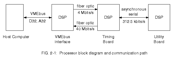
A typical system will have a total of four processors that need to communicate with each other - the host computer, the VME or SBus host computer interface board, the timing boards and the utility board. The VMEbus interface has a DSP, while the SBus interface board has a special purpose chip made by LSI Logic to execute direct memory access cycles on the SBus, called the DMA+ chip. The timing and utility boards have DSPs. The boards communicate along a linear path, as shown in Fig. 1-2, wherein a command sent from the host computer to the utility board must pass through the
A communications protocol has been implemented in the DSP code that recognizes that three types of data exist - commands, replies, and image data. Commands and replies are multi-word, short strings that are passed between any of the four components of the system, whereas image data can only be passed from the timing board through the interface and on to the host computer. Commands and replies always contain a header in the first word, formatted according to:
Source byte, destination byte, number of words in command
This is a three byte word, which fits nicely into the 24-bit data word length of the DSP, and source and destination designations are assigned to each of the four processors as follows:
	0	Host computer
	1	VME interface board
	2	Timing board
	3	Utility board
The number of words in the string can be from two to seven, and the header is counted as one word. Command and reply strings contain three byte ASCII strings, all upper case, in the second word. Some commands are followed by one or more numbers whose meaning depends on the command. Replies always contain two words total, the header and the reply. For example, the command for the host computer to write a NOP instruction to the Utility board P: memory in the $78'th location is:
$000304 'WRM' $100078 $000000The utility board will respond to the host computer with a reply:
$030002 'DON',
meaning that the indicated command was executed satisfactorily. The $1 in the most significant nibble of the address field of the WRM instruction is an encoding scheme to indicate the P: (program memory) is to be updated; X:, Y: and ROM data memory can also be accessed.
A hiearchical philosophy has been adopted in partitioning which boards perform which time critical tasks. The most time critical tasks of CCD readout timing and voltage control are performed by the timing board which operates on a time scale of order one microsec. Similarly, the VME or SBus interface board performs time critical tasks limited to data handling on a microsec time scale . The utility board is next in the hierarchy, performing tasks on a time scale of order one millisec. Non-time critical tasks are performed by the host computer. Paralleling this hierarchy, the microsec time scale boards are capable of only limited error checking and reporting and rely on other system components to manage them. The utility board performs modest error checking and reporting, and initiates timing and VME interface board operations. Finally , the host computer performs extensive error checking and reporting on a non-real-time basis, and directs the utility board to manage time critical operations. As an illustration, the sequence of commands needed to execute a normal timed and shuttered exposure with a VMEbus interface board is:Host writes exposure time to utility $000304 'WRM' $400018 time Host writes # of columns to timing $000204 'WRM' $400001 #cols Host writes # of rows to timing $000204 'WRM' $400002 #rows Host writes number of pixels to VME $000104 'WRM' $200007 npxls Host sends start exposure command to Utility $000302 'SEX' Utility sends clear CCD to timing $030202 'CLR' When done, timing send done clear to utility $020302 'DON' Utility opens shutter, starts exposure timer internal utility board operations When timer elapses, utility closes shutter, sends start readout command to VME interface $030102 'RDC' Utility send start readout command to timing $030202 'RDC' VME sends done reply to host when $010002 'DON' readout complete
The timing board sends image data to the VME interface, which writes it first to on-board buffer memory then to the VMEbus. Similarly, the SBus interface board writes data first to on-board FIFO memory, then to medium-sized system buffers, then to the final large image in user memory space. When npxls have been sent the timing board re-enters either the idle mode or the stop mode depending on whether a 'IDL' or a 'STP' command was last issued, and the VME interface enters command interpreting mode.
During readout the VME and SBus interface boards interprets all data coming from the timing board over the fast fiber optic data link as being image data. Both the interface board and the timing board are still looking for commands to allow the host computer to abort the readout in progress if needed. Proper management of the readout parameters is assumed by the host computer, but any task requiring time critical service is initiated by one of the DSP boards.
An initialization procedure is needed after system reset. Because the procedure is not time critical and requires a modest degree of checking to insure that it is completed successfully, it is performed by the host computer:
	Test system:		$000103 'TDL' number	reply:    $010002 number
			$000203 'TDL' number	reply:    $020002 number
			$000303 'TDL' number	reply:    $030002 number
	Load VME program	$000103 'LDA'  2	reply:    $010002 'DON'
	Load timing program:	$000203 'LDA'  2	reply:    $020002 'DON'
	Load utility program:	$000303 'LDA'  0	reply:    $030002 'DON'
	Turn on analog power:	$000302 'PON'	reply     $030002 'DON'
The commands will reply with 'DON' after completing command execution, if successful. Further system checks after this initialization procedure completes can be made by reading the values of the analog voltages from the utility board Y: data memory table with the 'RDM' command, and performing additional 'TDL' tests after full system initialization.
To control and read out detector arrays the timing board generates digital signals that are bussed over the backplane to one or more clock driver boards and one or more video processor boards. On the clock driver board these signals are connected to analog switches that select high or low voltages that are input to op amps that connect to the clock lines of the array. On the video processor board some of these signal connect to analog switches performing the signal processing, and others to the A/D converter to issue a start conversion pulse and to a latches to store the A/D data. These timing signals are generated by having the timing board write from internal memory to latches on the timing board that drive the lines SS0 to SS15. These are" switch state" signals, with SS0-11 controlling the switch states and SS12-15 used as board select so multiple clock driver and video processing boards can be used in a system. There is a strobe signal TIM-A-WRSS that undergoes a low-to-high transition when the data lines SS0-15 are valid. Careful attention has been paid to provide reliable operation with a large and variable number of boards in the system by having the signals SS0-15 valid for the entire 40 nanosec instruction cycle, by using high current bus driver (from the TI ABT series), by placing the TIM-A-WRSS strobe signal at the center of the time that SS0-15 are valid, and by keeping the receiver latching circuits on the clock driver and video processor boards close to the backplane connector to minimize signal rise times. Placing more boards in the system increases the rise time of TIM-A-WRSS and SS0-15 due to increased inductive loading by the signal traces of the added boards. A measurement with 3 boards installed was extrapolated to estimate that the increased delay time will be 10 nanosec with 20 board installed, well within the reliable operating range of 40 nanosec.
To write a number to update the switch states one simply writes the desired number to the memory location X:$FF80, as follows -
	MOVE	#$ddbsss,A	; Write switch state sss to board #b with delay dd
	MOVE	A,X:$FF80	; Write this number to the WRSS memory mapped location
The bits are encoded as follows -
	D16-D23	dd	Delay execution of the next instruction by the following
		If D23 = 0 then delay by D16-D23 steps of 20 nanosec, plus 80
nanosec
		If D23 = 1 then delay by D16-D23 steps of 160 nanosec, plus 80
nanosec

	D12-D15	b	Board select number, which should match the "SWITCH"
 jumper setting of either a clock driver or video board

	D0-D11	sss	Switch state bits
Two modes of reading image data from the video processor to the timing board are implemented - through the DSP and through a PAL. The DSP can simply read the A/D counts from any one of 32 A/D converters in the system and write it to the fiber optic transmitter with the instruction
	MOVE	Y:$FFA1,A		; Read A/D #1 into accumulator
	MOVE	A,Y:$FFC0		; Write accumulator to fiber optic
transmitter
The A/Ds are memory mapped over the range of Y:$FFA0 to $FFBF. Each of these instructions executes in one DSP instruction time plus one wait state, or 120 nanosec for the two instructions.
An alternative method of reading the A/D counts is to utilize a PAL circuit on the timing board that generates the addresses of the A/Ds to be read from a starting value to an ending value, each of which can be from 0 to 31. The circuit passes the A/D values to the serial transmitter as well, so the DSP only needs to initialize the circuit. This is done by having the DSP write as follows, where the notation % indicates that the word is written in bit, rather than nibble, fashion -
	MOVE	#%dddddddd1111xxeeeeebbbbb,A	; Read A/D numbers 0 to 4
	MOVE	A,X:$FF80			; Write this number to the PAL
The address X:$FF80 is the same one used to write switch states allowing this instruction to be placed in a clocking waveform for minimum overhead. The bits of the data word are encoded as follows -
	D16-D23	dddddddd	Delay, normally not used here
	D12-D15	1111	Must be set to $F for this circuit to execute
	D10-D11	xx	Not used
	D5-D9	eeeee	Ending A/D number
	D0-D4	bbbb	Beginning A/D number
For example, MOVE #$00F060,A will read and transmit the A/D values from a quadrant readout system, that is. A/Ds 0 to 3. The beginning and ending numbers can be equal, can range over 0 to 31, but the ending number must be greater than or equal to the beginning number.
There are DACs on the clock driver board that set the high and low voltages between which the clock switch, and on the video processor board for setting DC bias voltages for the detector arrays and offset voltages within the video processor. The DACs are loaded with digital numbers that are generated by the synchronous serial interface (SSI) circuit of the timing board DSP and transmitted to each DAC by a serial data stream that is decoded by PALs (Programmable Array Logic) on each board. The serial data is sent in 24-bit words, most significant bit first, at a speed of 4.17 Mbits/sec. The 24-bit data word is decoded by the clock driver and video processor boards as follows -
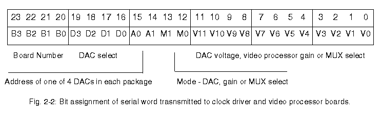
B3 - B0 Selects the board number that is to be written to. The clock driver and video processor boards have four jumpers headers labeled "DAC address" that need to match the bits in the serial word for the board to accept it. The jumpers are installed to set the bit to zero. Up to 32 clock driver and 32 video processor boards can be addressed in a system.
D3 - D0 Selects the DAC package number to be written to. There are twelve DACs on the clock driver board that are selected by numbers D = 0 to 11, and four DACs on the video processor that are selected by numbers D = 12 to 15. Note that clock drivers and video processor boards can have the same board select number. The Mode bits below must be zero (M0=M1=0)to write to a DAC. If D2 = D3 = 0 then the V bits will set the MUX address. If D2 = D3 = 0 then the V bits set the video processor gain.
A0 - A1 There are four DAC circuits in each package, and these two bits simply select which of the four is to be written to. M0 - M1 Mode bits to select between DAC writes, gain select on video processors and output multiplexer (MUX) select on the clock driver board. M0 = M1 = 0 to write to a DAC M0 = M1 = 1 to select a gain or a MUX according to bits D2 and D3.
V0 - V11 The 12-bit digital number written to the DACs to select its output voltage, if writing to a DAC. If the video processing gain is selected then V0 to V3 sets the gain of channel 0 and V4 to V7 of channel #1. If the MUX is selected then they select which of 24 clock driver circuits are connected to the diagnostic connector for examination with an oscilloscope.
A facility exists for resetting the DSPs in a variety of ways. Restting DSP is accomplished simply be bringing its REST* pin low, which causes the DSP on the timing board to read the initializing boot code from on board ROM and the DSP on the utility board to start executing ROM code directly. After a reset the DSP executes the boot code, but the application code is lost by the reset . Several mechanisms exist for the timing board DSP to reset, as follows -
(1) Power-on: A power monitor circuit asserts the reset line several hundred milliseconds after the +5V power Vcc is applied.
(2) Host fiber optic command: If the bit pattern $53xxxxxx is sent by the host computer the serial reciever PAL will issue a DSP reset. This may be useful to remotely resetting the DSP in cases where it is no longer executing commands correctly.
(3) DSP software command: The command 'RST' will cause the DSP to enter the reset state.
(4) Power control board reset switch depression: The reset switch on the power control board can be pressed to generate a low signal on EXT-T-RST which will get passed over the backplane to cause the timing board to reset.
(5) Power supply reset switch depression: The large black pushbutton on the power supply is passed on the power supply cable to the power control board to reset via the EXT-T-RST signal.
Whenever the timing board is reset it will execute a short routine that asserts the TIM-U-RST line that is passed over the backplane to the utility board to reset it. The utility board will be reset by its own power-on circuit, by pressing its own reset switch, by its own watchdog timer circuit (it enabled) or by this timing board signal.
There are maximum numbers of both clock driver and video processor boards that can be installed in the system, as determined by logical addressing limits. There is a maximum of 21 boards total that can be installed in a VME backplane, which is just the maximum number of slots in the VMEbus specification. There are other limits imposed by controller size and power dissipation, but this section deals only with the logical addressing limits.
The logical addressing limit for the number of A/Ds in a system is set by the number of signals TIM-ADADR# which are used to address the desired A/D value. TIM-ADADR runs from 0 to 4, so a maximum of 32 A/Ds can be put in a system, or 16 dual readout video processor boards.
Similar, but more complex, limits are set by the number of switch state and DAC board address bits, as follows. There are four address bits (D12-D15) encoded in the switch state word, but one of these ($F) is reserved for the series transmit (SXMIT) function, so fifteen board addresses are available. Each clock driver board has two board addresses, one accessing the bottom 12 clock drivers, and one accessing the top 12 clock drivers. Therefore, 15 clock driver half boards, or 7.5 clock driver full boards, may be separately accessed with different timing instructions. The switch state circuits are designed so that several clock driver boards can be jumpered to the same switch address so they have the same timing. This is useful in mosaic applications where several detector arrays have the same geometry and the timing needs to be done strictly in parallel for all the arrays in the mosaic.There is no limit for the number of clock drivers with the same board address. Similar considerations apply to the number of video processing boards, though only one switch address is used per board. Because the clock driver and video processor boards utilize the same switch state address field the number of separately addressed video processor boards plus clock driver half boards is 15.
The serial transmitter word that is sent to all the boards to write numbers into the DACs contains a four bit board number address field, and is used for both clock driver and video processing boards. Each DAC board address writes to all the DACs on an addressed clock driver or video processing board, not two addresses per board for the timing data. Also, the board addresses are set up differently for clock driver and video processing boards, so a total of 16 clock driver and 16 video processing boards may be installed in a system. At 24 clocks per clock driver board this works out to a maximum of 384 clocks per system and 32 A/D converters.
To summarize -
	Max. number of video processing boards		16
	Max. number of clock driver boards		16
	Max. number of differently timed video processor boards
	    plus clock driver half boards		15

	Fiber Optics Serial Protocol

	Required care with fiber optic connectors
		Use plastic connectors on fiber optics cables
		Use bayonet couplers
		Be careful

	Compatibility with Gen I components
		Utility board is fully compatible with ROM change
		Power control board is compatible with PAL change and two added
wires if reset functions are desired - RECOMMENDED
		Host interface boards are compatible with reduced image transfer
 speed, about a factor of 2. Different PALs required in timing board- ??
		Controller housing, power supply fully compatible
		New timing, video processor and clock driver boards required -
old analog boards will NOT work with new timing board, and vice versa.

	Power Distribution
		+/- 16V from PS regulated to +/- 15V, +/- 5V on video board,
 			+/- 12V on clock driver
		+5V not regulated anywhere
		Cable drops the voltage so user should check it on controller
boards, esp. 5V
	OnCE Port in-circuit emulator for DSP debug on timing board
		->  How to purchase

	DSP software toold - Motorola assembler
		->  How to purchase
The first generation controllers are usable for a variety of both optical and infrared image sensors and have been operated by a number of groups worldwide. Below is a list of the types of sensors known to be operated by each institution, with apologies requests for corrections to groups who are listed incorrectly or incompletely:
Miscellaneous Loral Back to Document List Page.