
This chapter has been updated to describe circuit board Revision 6B, the current revision of the DSP software 2.31.
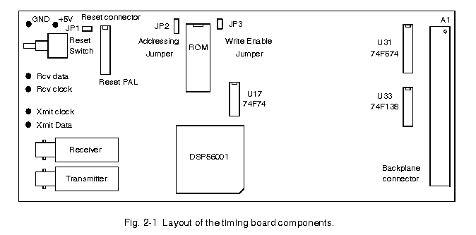
The principal components of the timing board are shown in Fig. 2-1. The connector JP1 near the reset switch allows connection of a remote switch for resetting the DSP, and should never have a jumper installed on it. Fig. 2-2 describes the meaning of jumpers JP2 and JP3, and the EEPROM memory map.
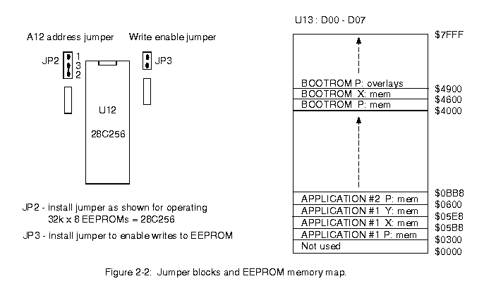
Versions 2.10 and later of the DSP software can only be executed from 32k x 8 EEPROMs (28C256). 8k x 8 UV erasable ROMs will still work with these timing boards, but only with earlier revisions of the DSP software. The address selection jumper JP2 should be set as shown in Fig 2-2 for operation with 32k x 8 EEPROMs. A jumper should be installed on JP3 if the user needs to write to the EEPROM while it is installed in the timing board. Hardware protection of the EEPROM contents can be provided by not installing the write enable jumper. Software protection is provided against writing to the boot area of the EEPROM by disallowing writing above address $4000. This prevents damage to the boot program so basic DSP operation, memory management and communication functions will be operational after the DSP is rebooted even if erroneous writes to the DSP or EEPROM application program have been made.
A procedure for checking out the operation of the timing board is outlined here, to be used if a previously functional board is suspected of improper operation, or for initial tests after board assembly. The checkout steps are as follows:
(1) Visually inspect the board: The correct ROM should be installed, and the socketed components (DSP and EEPROM) should be properly installed and seated. JP1 should not have a jumper. The jumpers JP2 and JP3 should be correctly installed as described above. The resistors should all be installed.
(2) +5 voltage supply: Before plugging in the board check the resistance between +5V and ground, using the test points in the upper left hand corner of the board. It should be around 3k ohms after it settles down. Turn power on, verify that the voltage goes to +5 volts.
(3) Power-on reset: Examining the EEPROM chip enable (U13 pin #20), the +5V power to the timing board should be cycled on and off several times. The chip enable line should toggle for about 5 milliseconds after reset as the boot program is loaded into the DSP and then remain in a high state. The reset switch should be pressed to produce the same effect as power-on reset.
(4) External clocks: The 8 MHz clock should be examined at the backplane connector on pin A10, and should be high for 75 nanosec and low for 50 nanosec. The 20 MHz clock should be on the backplane pin A12, and should be symmetric.
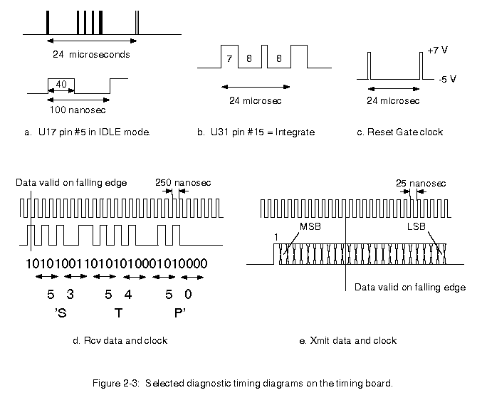
(5) Computer communication: With the timing board connected to the host computer via the optical fiber link, several commands should be issued. Examining U17 pin #5 with a scope, a STP command should stop the waveforms, an IDL command should resume them, and a RST command should produce waveforms like the power-on reset. The TDL command should be executed to verify that the serial link works in both directions. The STP command should be sent repeatedly from the host computer with a scope connected to the Rcv data and Rcv clock pins, as shown in Fig. 2-1, to obtain the waveforms shown in Fig. 2-3d.
(6) Verify DSP operation: The 74F74 flip flop U17 can be examined with a scope to see if the DSP is cycling through the IDLE routine properly. Pin #5 should reveal the waveform shown in Figure 2-3a.
(7) External clock waveforms: The commands LDA #2 and IDL should be executed to load the dual readout application program and activate clock driver activity. A spot check of a signal on U31 should be made by examining pin #15 with a scope. It should appear as in Fig. 2-3b. This is the signal that turns the integrator of the video processor on and off.
(8) Clock driver waveforms: An analog board should be plugged in, and the clock driver waveforms should be examined from the DC37 connector that connects to the CCD. Pin #8 has the Reset Gate signal that should appear as in Fig 2-3c.
(9) DSP code downloading: An operational DSP program should be downloaded from the host computer to the DSP memory over the fiber optic data link.
(10) Image data transmission: A CCD image should be read into the host computer with the RDC command while a scope is placed on the Xmit data and Xmit clock pins shown in Fig. 2-1. The waveforms of Fig. 2-3e should be obtained.
Once these steps are satisfactorily completed the timing board has a good chance of being fully functional, and a readout of a CCD image could be attempted.
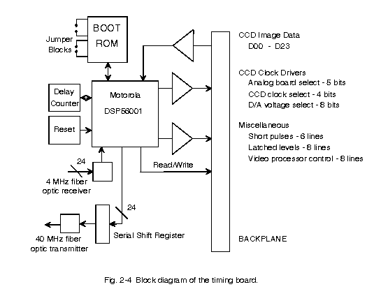
Fig. 2-4 shows a block diagram of the main components of the timing board. A boot ROM loads the DSP with its program and parameter set after power-on reset or an explicit command from the host computer, while a hardware delay circuit stops the DSP from executing commands for programmable intervals. Buffers to the backplane implement a range of programmable timing pins and receive image data from each of the analog boards. A detailed description of the operation of the timing board follows, and makes reference to the board schematic.
The DSP (DSP56001, U20), its boot ROM (U13), power-up logic (surrounding the reset switch in the lower left hand corner) and the 40 MHz master timing clock (U5) are shown in the drawing. The ROM contents are loaded into the DSP program memory space by a bootstrap loading program resident in he DSP. This occurs during the reset cycle just as RESET* (pin A5 of the DSP) is brought high. D23 of the DSP is held high by R5 to signal to the DSP that the boot program is on the external bus in a ROM, causing the DSP to go through a read cycle over the byte-wide data bus lines D0-D7. The entire on-chip program space of 512 words is read in, as the DSP sends its program strobe PS* line true together with its read external memory RD*. These map directly to the ROM lines chip enable CE* and output enable OE*. Jumper JP3 is for ROM protection to prevent unauthorized writes.
A reset signal for the DSP is generated by a programmable array logic (PAL) part U1. Its logical equation is
| RESETI = (SYSRST' # RESW')' |
| IRQA = RESETI' # IRQAIN |
| IRQB = RESETI & IRQBIN. |
where # means logical OR, & means logical AND and ' means logical invert. The DSP reset signal RESETI goes low whenever the bus signal SYSRST goes low or the on-board reset switch and power-on circuit sends RESW low (true). IRQA goes low and IRQB goes high during reset so the DSP reads an operating mode value of 2 to enter the special DSP56001 bootstrap mode. When RESETI is high IRQA and IRQB just follow the input interrupt request lines IRQAIN and IRQBIN respectively.
The crystal oscillator U5 runs at 40 MHz to generate the bit clock for the fast serial transmitter, and is divided by two by U8A to run the DSP clock input pin. U9 divides the 40 MHz clock to generate an 8 MHz clock that is bussed to external readout boards (backplane signal CK8) for use by the A/D converters, and is driven by U12C. U9 is cleared with a programmable PULSE2 signal in order to synchronize the clock with pixel readout. The PAL U1 puts the DSP in operating mode 1 after reset o that the DSP boots its program memory a byte at a time from the EEPROM U13. Reset circuitry is activated by either power-up or pushing the camera reset button S1. A remote reset switch can be wired to JP1.
The DSP generates external data bus reads or writes whenever memory data accesses outside of its on-chip memory space are performed. U10D is used in conjunction with the flip-flop U17A and a delay line U14A and U14B to produce a WRITE* signal of 40 nanosec duration if a DSP write command issued. This is driven by U16 to generate SWRITE, which is sent to the bus for use by other boards in the system for latching data values. The data lines D00-D23 are latched by U30, U32 and U35 from the DSP data bus when a DSP write command is issued to the external memory space, and they in turn drive the system bus lines SD00-SD23 and guarantee that the data values are valid during the SWRITE latching pulse. Similarly, an SREAD signal is generated when a DSP read operation is performed, causing the three state outputs of U30, U32 and U35 to be disabled as the drivers U25, U27 and U29 drive the DSP bus during a read instruction.
A delay logic circuit is implemented by U12B, U12D, U17B, U22 and U23 to allow a programmable number of clock cycles (0-255) to be inserted in-between DSP instruction execution, effectively halting all processing. The number of clock cycles to be inserted is programmed in the data word D16-D23 during writes by the DSP to X: external memory space. If these bits D16-D23 are all zero then no delay is inserted. The comparator U23 monitors D16-D23 and generates a low true signal if the bits are all zero. The flip-flop U17B checks these bits whenever STROBE* goes high and X/Y* indicates an X: cycle is in progress. If the bits are all zero then U17B's output Q* stays high, preventing the DSP bus request BR* from going true, and preventing the 8-bit binary counter U22 from counting. If any of the data bits are not zero then the D input to the flip-flop U17B will be high and Q* will go true. Q* true causes the bus request line BR* to be taken true, stopping DSP execution immediately until BR* is taken high after the counter U22 has counted down and cleared the flip-flop U17B. Each delay cycle is 50 nanosec, so 50 to 12750 nanosec delays are possible. The delay occurs after execution of the instruction containing the non-zero delay field.
The lower right hand corner of the schematic shows the fast serial transmitter. The transmitter accepts SD0-SD23 off the system bus whenever U18 goes true. This causes the bank of shift register U21, U24, U26 and U28 to enter parallel load mode, whereby the data are loaded on the next highgoing clock. The start bit of the 25-bit serial word is generated by the most significant bit of U28. After parallel load, U18 goes false to let the shift registers resume shift right operation as the bits go cascading from one device to the other. After transmission of the entire data word the shift registers go right on clocking, but send out all zeroes since the input SR to the first shift register in the line U21 is set to zero. The serial stream simply goes to the optical transmitter U4 to be sent down the optical fiber to the instrument control computer. The shift registers are reset on SYSRST* and clocked out by the system clock at 40 MHz. The serial encoding over the fiber is scrambled by the serial transmitter, and seen as NRZ by the on-board circuitry. Input data arriving at 4 MHz is received by the optical receiver U3 and sent to the clock recovery chip U2 for it to generate a synchronous clock. This synchronized clock and the serial data stream are sent to the DSP Synchronous Serial Interface (SSI) pins for writing to its internal 24-bit input register. The counter U7 in conjunction with U8B and U12A generates a status signal to tell the DSP when the data is valid. The delay line U14C insures that the clock occurs right before the data transition so phasing errors do not occur.
Provisions for communicating with the serial interface of the DSP are provided. The asynchronous serial interface transmitter (TXD) and receiver (RXD) lines of the DSP (the SCI) are wired to the backplane to allow communication with another processor. The synchronous serial transmitter lines, STD and SCK, are provided to allow the DSP to transmit data, and are buffered through U10A and U10B to allow more than one receiver to hang on the line.
The bank of four circuits U19, U31, U33 and U34 handles a miscellany of utility and support functions. The comparator U19 selects these functions whenever an external X: memory write is made with SD12-SD15 set to ones ($F). Three different kinds of signals are generated. The latch U31 and decoder U33 assure that the VP lines 0-7 are updated simultaneously with the contents of SD00-SD07 whenever SD08-SD11 are zero. The analog readout boards currently use these lines for running the video processors of all readout boards in parallel. The lines PULSE3-7 generate a low-true pulse of 40 nanosec duration whenever a write is made to X:$FFB0 with the data word $00Fpxx, where p = 3 to 7 selects which of the PULSE lines to toggle. Lastly the addressable latch U34 generates latched signals that can be individually addressed by writing to the same X:$FFB0 address with the data word $00F1xn, where the three most significant bits of n will address the lines LATCH*0-7 and update the indicated one to the value of the least significant bit of n.
The driver U16 is always enabled to drive the address lines A00 to A03 and control signals READ*, WRITE*, X/Y* AND Y/X* with sufficient current over the bus. These bussed signals are indicated with an S prefix, as in SREAD. The address lines A00 to A03 are used to address each analog board to read each A/D converter separately. The X/Y* and Y/X* signals are generated by the DSP for addressing either the X or the Y data memory space, and separately bussed for ease of decoding by the readout boards. U15 latches the memory select signals X/Y and Y/X and the address lines A00-A03 to insure that they are valid after the termination of the DSP write cycle, and sends them out over the bus with an L prefix.
A summary of the DSP commands follows. A non-zero in the mm fields will cause the next instruction execution to be delayed by (mm times 50 nanosec). x means "don't care".
| MOVE | #$mmF0nn,X:$FFB0 | Write nn simultaneously to all VP lines 0-7. |
| MOVE | #$mmF1xn,X:$FFB0 | Update LATCH 0-7 to the value of the least significant bit of n. The three most significant bits of n select which of the eight LATCH lines to update. |
| MOVE | #$mmFpxx,X:$FFB0 | Generate a 40 nsec pulse on one of the PULSE lines p = 2-7. |
| MOVE | #$mmnopp,X:$FFB0 | Write to the external board selected by n (n = 0 to $E). If an analog board, update its o'th DAC to the value pp. |
| MOVE | #$mmnopp,X:$FFB1 | An additional 16 external boards may be selected. |
| MOVE | A,Y:$FFB0 | Transmit the 24-bit value in accumulator A over the fast (40 MHz) serial link to the host computer. |
| MOVE | X:$FFBq,A | Read the A/D of board q into accumulator A; q = 0 to $F. |
| MOVE | Y:$FFBq,A | An additional 16 A/Ds may be read; q = 0 to $F |
The pins of the backplane have been defined as follows -
| Pin # | ROW a | ROW b | ROW c |
|---|---|---|---|
| 1 | VP0 | RXD-U | SD00 |
| 2 | VP1 | TXD-U | SD01 |
| 3 | VP2 | PWREN | SD02 |
| 4 | VP3 | *UTLRST | SD03 |
| 5 | VP4 | *USER | SD04 |
| 6 | VP5 | *USER | SD05 |
| 7 | VP6 | *USER | SD06 |
| 8 | VP7 | *USER | SD07 |
| 9 | GND | *USER | GND |
| 10 | CK8 | *HVEN | SD08 |
| 11 | GND | *USER | SD09 |
| 12 | CK-20 | LX/Y | SD10 |
| 13 | PULSE3 | LY/X | SD11 |
| 14 | PULSE4 | LA00 | SD12 |
| 15 | GND | LA01 | SD13 |
| 16 | PULSE5 | LA02 | SD14 |
| 17 | GND | LA03 | SD15 |
| 18 | WATCHDOG | RXD | SD16 |
| 19 | GND | TXD | SD17 |
| 20 | IRQU | GND | SD18 |
| 21 | *LVEN | SCK | SD19 |
| 22 | *PWRST | STD | SD20 |
| 23 | SC0 | GND | SD21 |
| 24 | SRD | IRQA | SD22 |
| 25 | LATCH2 | IRQB | SD23 |
| 26 | LATCH3 | IRQB-U | SREAD |
| 27 | LATCH7 | SWRITE | SX/Y |
| 28 | LATCH6 | SY/X | SA00 |
| 29 | LATCH5 | SA01 | SA02 |
| 30 | LATCH4 | SA03 | SYSRST |
| 31 | VS- | VHS+ | VS+ |
| 32 | +5 VDC | +5 VDC | +5 VDC |
The power supply delivers +5, +/- 15 and +36 volts to the controller, the first three through the dedicated power distribution pins on the VME backplane. The +36 volts for the DC bias supply is delivered through the VHS+ pin (b31). Normally it is expected that the power supply will be mountedremotely from the controller some distance away. Noise pickup along the power supply cables can be minimized by proper bypassing or re-regulation at the controller, while the extensive on-board regulation provided by the noise-critical analog readout boards should minimize its effect. Signals names preceded with an asterix (*) are daisy-chained on standard VME backplanes, rather than bussed to all connectors. Some are dedicated to the utility board and go between it and the power conditioner board, necessitating that the utility board be placed in either slot 0 or slot 6 in systems equipped with a power conditioner board, or that the VME backplane be jumpered between the desired pins. A short description of each signal follows:
VP0-7: These eight signals are updated simultaneously with a MOVE #$mmF0nn,X:$FFB0 instruction. They are all mapped to the video processor pins on the analog board.
PULSE2-7: These six signals, individually addressable, send a 40 nanosec low true pulses onto the bus when a MOVE #$mmFpxx,X:$FFB0 instruction , p = 2 to 7, is executed.
LATCH0-7: These eight signals, individually addressable, can be each set to be maintain a high or low value until explicitly changed. MOVE #$mmF1xn,X:$FFB0 addresses each of the eight signals according to the value of the three most significant bits of the n nibble.
USER: The user may use these backplane pins freely. Some of them are not bussed, but are daisy-chained from one board to the next.
RXD, TXD: These are connected directly to the DSP asynchronous serial interface pins, for communication between the utility board and the timing board.
SCK, STD: These are buffered transmitter and clock outputs from the DSP synchronous serial interface.
IRQA, IRQB: These are interrupt request inputs to the DSP, and go directly from the bus to the DSP.
GND: Digital Ground.
+5 VDC: This is the digital power input from a user supplied power supply.
CK8, CK20: These are clock outputs from the timing board at 8 and 20MHz. The 8 MHz clock is software selectable to be synchronized with pixel processing, and the 20 MHz clock is synchronized with DSP instruction execution.
WATCHDOG: Connected to PULSE6 on the timing board this line is monitored by circuitry on the utility board to make sure the timing board is alive.
HVEN, LVEN: These low true lines allow the utility board to instruct the power conditioner board to turn on and off the indicated power supplies (high voltage, nominally +36V, and low voltage, nominally +/- 15) during the power-on sequence to protect the CCD from turn-on transients.
PWREN: This line allows the utility board to instruct the power conditioner board to turn on the low voltage lines (nominally +/- 15V) to an intermediate value so the analog circuits can become stable. As a sanity check it must be toggled 128 times to do this.
PWRST: Asserting this low true line will reset the power enable counter on the power conditioner board. It also immediately drops the analog voltages to zero.
RXD, TXD-U: This line connects to the asynchronous serial receiver and transmitter lines of the utility board for connection to external devices.
IRQB-U: Asserting this line will interrupt the utility board processor.
LX/Y, LY/X: These are latched versions of memory space indicators SX/Y. They are guaranteed to be valid through the SWRITE latching signal. LX/Y is high when an X: memory cycle is in progress, and LY/X is its inverse.
LA00-LA03: These are address lines from the DSP, and latched to be valid during the SWRITE and SREAD latch signals.
SWRITE: This is a pulse that goes low for 40 nanosec and indicates that a DSP write cycle is in progress. The data lines SD00-SD23, address lines LA00-LA03, and memory space lines LX/Y and LY/X are all valid. Executing the DSP instruction MOVE #$mmnopp,X:$FFBq toggles SWRITE and is used to write data values to the DACs on the analog board.
SX/Y, SY/X: These are high current versions of the X/Y signal generated by the DSP. They are unlatched, as opposed to LX/Y and LY/X. SX/Y indicates an X: memory access is in progress, and SY/X is its inverse.
SA00-SA03: These are high current versions of the four least significant DSP address lines.
VHS+: This supplies power for the high voltage unipolar DC bias supplies on the analog board. It is nominally +36 volts.
SD00-SD23: These are the complete data lines to and from the DSP. They are read/write lines, and are buffered by high current latched drivers on write cycles, and a received by a three-state receiver on read cycles.
SREAD: This signal indicates that a read cycle is in progress. It is 40 nanosec long, low true. It is normally used to read the A/D converters on the analog board. Executing the DSP instruction MOVE X:$FFBq,A or MOVE Y:$FFBq,A (q = 0 to 15) will assert this line.
SYSRST: This line is a low true signal generated by the reset circuit on the timing board that is asserted whenever the DSP is reset, whether by power on or by manually pressing the reset switch. It can also re asserted by any board on the bus, and is used by the utility board to reset the timing board as needed.
UTLRST: Asserting this low true line will reset the utility board and reboot its DSP. It is intended to be asserted by the power conditioner board when the +5V digital supply turns on.
This document describes the DSP program contained in the timing board DSP application programs dealing with CCD readout. The commands discussed in the system chapter (RDM, WRM, LDA, RST and TDL) are also implemented. The boot program is contained in a file named "timboot.asm". Several application programs are also written. These have several commands in common as follows.
RDC - "Read CCD". Immediately read out the CCD. The entire image will be read out according to the constants contained in the following memory locations:
| Y:1 | Number of pixels per line. |
| Y:2 | Number of lines. |
| Y:3 | Number of pixels to clear from the serial shift register before image readout. This will typically be five times the number of pixels in the serial shift register (default = 5220). |
| Y:4 | Number of lines to clear before exposing. |
| Y:5 | Binning factor in the serial direction. |
| Y:6 | Binning factor in the parallel direction. |
STP - "Stop idling". Exit idle mode and leave the clocks not clocking.
IDL - "Start Idling". Put clocks in the readout sequence but don't transfer a ny data. Once the idle mode is entered by executing this command the camera will idle after executing any other command, except stop, which causes the idle mode not to be entered.
RAD - "Reset A/D". This resets the A/D converters by going through their self-calibration cycle. It takes 1.5 seconds. It should also be executed after analog power is turned on, and periodically to maintain calibration, especially if the temperature of the analog board changes significantly.
CLR - "Clear". This clears the image from the CCD by executing Y:4 (default = 5120) parallel clock shifts. It should be done before an exposure.
OSH - "Open Shutter". Open the shutter by sending out a LATCH1 = 1 signal. The utility board has circuitry that is better suited to controlling a shutter, so this command is being maintained in the timing board for backwards compatibility.
CSH - "Close Shutter". Close the shutter by sending out a LATCH1 = 0 signal.
SBV - "Set Bias Voltages". This will write the voltage codes in the appropriate Y: data memory area to the DC bias digital-to-analog converters.
HGN - "High GaiN". Set the analog boards to the high gain configuration.
LGN - "Low GaiN". Set the analog boards to the low gain configuration.
The file "tim1.asm" is assigned application number 1 for loading into EEPROM, and is a single readout application. "tim2.asm" is a dual readout application with an application number of 2. As of this writing the tim1.asm file has not been optimized for readout speed, but tim2.asm has. Both are fully operational, but "tim1.asm" has a rather slow readout time of around 45 microsec per pixel for a single readout, compared to 25 microsec for the dual readout of "tim2.asm".
These commands require no arguments. They all generate a DON reply to the board that issued the command, except for the readout command RDC that only generates pixel data that is sent along the fast fiber optic link.
The file "timtest.asm", assigned application number 10, contains three commands for testing the system. Two of these (TCK and TDC) generate ramps on the clock driver and DC bias supply outputs and should NEVER be executed if an analog board is connected to a CCD. The third command, RDC, can be executed with a CCD connected. The commands will be executed by the DSP as it gets to them from a circular buffer for commands in the DSP that is 32 words long, so fairly lengthy sequences of commands may be sent at once. The commands are as follows:
RDC - "Read CCD". Generate a test image that starts with a 1 in the first pixel and increments the value in each pixel by one each time pixel data is sent. It circulates modulo 2**16.
TCK - "Test ClocK drivers". Generate a ramp on all twelve clock drivers of analog board #0.
TDC - "Test DC bias supplies". Generate a waveform on all seven DC bias supply DACs on analog board #0.
The following changes were made to the boot file timboot.asm making the transition from Rev. 2.25 to 2.30 software. Several new application programs were introduced, and several were renamed.
(1) SCI receiver ISR was compressed by eliminating duplicate instructions by changing program flow. The Status Register SR is now saved and restored.
(2) The Debug routine was eliminated.
(3) Move overlay area from $1D0 to right on top of boot code.
Application area now runs from $E8 to $200, not $1D0. The maximum application size is now $200 - $E8 = $118 words. Impact - the maximum Y: memory size on ROM is $B8 = 184 instead of 256 that would be possible if 3 x $256 blocks of EEPROM were assigned to each application.
Several applications programs are supplied in Rev 2.30, and are identifiable by their names or their application number. Some features - binning, sub-image readout and MPP operation - are implemented in some applications but not in others. This does not reflect any fundamental limitations of the controller nor any particular rhyme or reason, as users are encouraged to design applications to meet their particular needs by combining features from several programs. All the programs define the clock voltages to the same values, and are optimized for operation of a Loral 1024 x 1024 device thinned by SAIC.
This does single readout in the simplest possible manner - no binning, no sub-images. The parallel clocks are set up for full MPP (multiple phase pinned) operation wherein all parallel clocks are set to low voltages so they are inverted, both during image integration and readout as well. This reduces dark current by a significant amount.
This does two readouts from a single CCD assuming that they are located at opposite corners. Binning is supported. Because it is a multiple readout application the assembler directive line parameter REV4C must be defined to indicate whether or not a revision level 4C VME interface board is connected to the timing board. MPP has not been implemented for this application, but can be seen in the tim1 code.
This does four readouts, one from each of the corners of a single CCD. The parameter REV4C must be defined. Neither binning, sub-image nor MPP is supported.
Sub-images from a single readout can be read out with this application. Binning and MPP are fully supported. The skipping parameters are defined as follows:
| Y:7 = NPSKIP | Number of lines to skip before read |
| Y:8 = NSSKIP | Number of columns to skip before read |
| Y:9 = NSSKIP2 | Number of columns to skip after read |
The NSSKIP2 is somewhat redundant, but for now it must be set correctly.
This application will read up to about 70 regions of interest dispersed throughout the CCD image plane. The regions is set by the number of rows and columns parameters described above, and the position of the boxes is set by a table in the Y: memory space that is defined starting at the parameter NBOXES. Users should consult their assembly listing file to determine what this address is, since it is defined after all the waveform definitions. A significant limitation is that there may be only one readout box on any one line of the image. The first entry of the table is the number of boxes to be read out. After that there are three entries per box, where N is the index number of the box, starting at zero:
| Y:NBOXES + 3N + 1 | Number of rows to skip |
| Y:NBOXES + 3N + 2 | Number of left columns to skip |
| Y:NBOXES + 3N + 3 | Number of right columns to skip |
This is the test program described above, that should NEVER be executed with a CCD connected to an analog board.
 Back to Document List Page.