
CCD Controller
User's Manual
DISCLAIMER
The information in this document is believed to be reliable, though no
responsibility is assumed for inaccuracies. The San Diego State Astronomy Department
reserves the right to make changes to the products described herein to improve
reliability, function or design. Neither San Diego State University nor San Diego
State University Foundation assume any liability arising out of the application
or use of any of its products or circuits, particularly with regard to damage that
may occur in the operation of delicate and costly charge coupled devices (CCDs).
Bob Leach
- Dept. of Astronomy
- San Diego State University
- San Diego CA 92182
- (619) 594-1406
- FAX: (619) 594-7454
- leach@mintaka.sdsu.edu
Frank Beale
- Dept. of Astronomy
- San Diego State University
- San Diego CA 92182
- (619) 594-6674
GENERAL INFORMATION
The CCD (Charge Coupled Device) controllers designed by the San Diego State
University Astronomy Department consist of a set of electronic boards designed to
operate imaging CCDs in a slow scanned readout mode, wherein each pixel of the CCD
has its output signal sampled, filtered and converted to a 16-bit digital word
that is sent to the host computer. The controller design consists of four
different types of electronic boards supplied by San Diego State for controlling
a wide variety of CCD devices. These four boards include a timing board, an analog
readout board, a utility board/power control board combination and a VME interface
board.
This manual describes in detail the five boards, including hardware and software
preparation, system installation, theory of operation, and performance. To improve
the utility of this document, its chapters will be updated from time to time, and
the most recent revision date will be included on the title page. Backup copies
will be kept in an archival directory as significant changes are made. The revision
number of the software and circuit boards that is described will be listed at the
top of each relevant chapter.
Intended applications
The CCD controller is targeted to operating one or more CCDs or CCD readouts at
slow readout rates of up to 100k pixels per seconds. From one to 19 CCDs or CCD
readouts can be operated with one controller, though considerations of size, cost
and timing inefficiencies put a practical upper limit of eight or nine readouts.
The CCDs will normally be thermoelectrically or cryogenically cooled to reduce
thermal dark current generation. Considerable flexibility has been built into
the controller design to allow operation of a variable number of readouts, as
well as operation of a wide variety of CCD devices in such modes as staring,
drift scan, shuttered and frame transfer. The controllers can be programmed by
the user to meet a wide variety of applications, while several programs are
supplied to handle simple configurations and to provide the user with a starting
point in configuring their systems.
Performance
A list of salient performance parameters is presented below to give the user
some orientation. The meaning of some of the terms may not be apparent, but
hopefully some of this will get cleared up in the remaining sections of this
manual.
| Form Factors
|
| Timing board: | 3.96 x 9 inches (3U VME width only)
|
| Analog board: | 3.96 x 10 inches.
|
| VME interface board: | 9.2 x 6.30 inches (6U VME size)
|
| Utility board: | 3.96 x 9 inches.
|
| Power control: | 5.5 x 4.75 inches.
|
| Power Dissipation
|
| Timing board: | 1.27 A, 6.1 watts, +5 V only
|
| Analog board: | 8.15 watts total
|
| | +5V | 0.15 A, 0.75 watts
|
| | +15V | 0.31 A, 4.65 watts
|
| | -15V | 0.17 A, 2.55 watts
|
| | +36V | 6.5 mA, 0.20 watts
|
| Utility board: | 2.65 watts total
|
| | +5V | 0.3 A, 1.50 watts
|
| | +15V | 0.05 A, 0.45 watts
|
| | -15V | 0.05 A, 0.75 watts
|
| Power control board: | 1.65 watts total for four analog boards
|
| | +5V | 0.08 A
|
| | +15V | 0.04 + 0.004 A per analog board
|
| | -15V | 0.03 + negligible per analog board
|
Data path:
Fiber optic connection between timing board and VME
interface board. AT&T ST-type connectors, 62.5/125 micron multimode Ge-doped
silica core fiber cable.
The data words are 24 bits long, plus one start bit, with the most significant
bits first, NRZ scrambled. The VME interface board transmits at 4 Mbits/sec and
receives at 40 Mbits/sec.
DSP operation:
A Motorola DSP56001 Digital Signal Processor is
used as the heart of the timing board. It has an instruction time of 100
nanosec, and the following address spaces:
512 x 24-bit words program space.
256 x 24-bit words X: data space.
256 x 24-bit words Y: data space.
Approx. 60% of the program space, and 60 locations of Y: space, are used up
by the current program to control a dual readout CCD. Approx. 18-20 locations
of X: or Y: space are needed for each additional readout.
CCD Clock drivers:
Twelve CCD clock drivers are provided per analog
board. They each drive over the range of +10 to -10 volts, and provide 70 nanosec
rise and fall times, 10% to 90%, 20 volts transition. They can drive high capacitive
loads at approx. 30 milliamps typical drive current.
DC bias supplies:
Seven programmable DC bias supplies provide the following
voltage ranges:
One at 0 to +30 volts, intended for the Output Drain of CCDs.
Two at 0 to +20 volts, intended for the Reset Drain and general use.
One at -5 to +5 volts, intended for the Output Transfer Gate.
Three at -10 to +10 volts, intended for general use.
Their long term voltage stability is 5 millivolts, and their noise is less than
one microvolt rms if connected to the input of the video processor board.
Video processor:
A preamplifier operates at x10 gain, followed by a DC
restore circuit at a switchable gain of x2 and x4. A polarity reversing amplifier
drives a conventional resettable integrator to implement a dual slope integrator
that operates at unity gain at integration times of 8 microseconds. A driver and
level shifter supplies the A/D converter.
A/D converter:
16 bits, one's complement. 8 microsec conversion and 2 microsec
sample/hold times. A Crystal Semiconductors monolithic CMOS self-calibrating
successive approximation type converter is used.
Noise performance:
With the video processor input grounded, 0.98 ADU rms.
This is equivalent to 1.5 microvolts rms. A figure of 5.7 electrons rms was
obtained while operating a cooled CCD, the 1024x1024 CRAF/Cassini device, at a total
integration time of 16 microsec per pixel. The CCD had 1.0 microvolts per electron
node sensitivity. No degradation in readout noise was measured for the dual
readout case compared to single readout.
Readout Timing:
Readout at 23 microsec per pixel has been implemented for a
single readout with on-chip binning. A total of 16 microsec are spent integrating
on the CCD video (8 microsec on baseline plus 8 microsec on signal), while the
A/D sample/hold and conversion operations are fully overlapped with CCD clocking
and video processor functions with no increase in readout noise compared to
non-overlapped operation. Additional readouts add approx. one microsec to the
readout time.
Utility board:
A DSP56001 provides a miscellany of support functions for the
system, including integration timing, CCD temperature control, shutter control,
system power supply and temperature monitoring at a time resolution of one
millisecond. It also provides uncommitted analog and digital inputs and outputs
whose functions can be programmed by the user.
VME interface:
A DMA (Direct Memory Access) interface communicates between
the host computer and the timing board over the fiber optic data link. Once
initialized by the host computer it writes entire multi-megabyte images directly
to VMEbus memory, relieving the host processor of this real-time responsibility.
It has 32k x 24 bits of internal buffer memory, VMEbus interrupt capability and
32-bit data transfer capability, and contains a DSP56001 processor. Its transfer
over the VMEbus has been measured to be 7 Mbytes/sec.
System Description
The SDSU CCD camera controller simultaneously controls and reads out up to
19 CCDs at readout rates of up to 100k pixels per second. It can be used either
for operating many CCDs in a mosaic configuration, or for operating more than
one readout on each CCD in applications that require total CCD readout time to
be minimized, or combinations of these two configurations. The controller
supplies up to twelve clocked signals and up to seven DC bias voltages per readout
derived from a bank of digital-to-analog converters (DACs). The analog video
output of each CCD readout is amplified by low noise pre- and post-amplifiers and
filtered with a dual-slope integrator of programmable integration time before
being processed by a 10 microsecond conversion time Analog-to-Digital (A/D)
converter. A fully programmable Digital Signal Processor, the Motorola
 DSP56001, provides timing and clocking at a 10 MHz rate, and can be programmed
to control a wide range of CCD geometries and readout requirements. The control
ler accepts 24-bit commands from a user-supplied computer over a 4 Mbits/second
optical fiber data link, and supplies 16-bit pixel data over a 40 Mbits/second
optical fiber data link to the computer. A VMEbus interface card that contains
the required fiber optic connection and an intelligent DMA controller is under
development, as is a utility support board to handle functions such as CCD
temperature control, exposure timing, and system integrity monitoring.
DSP56001, provides timing and clocking at a 10 MHz rate, and can be programmed
to control a wide range of CCD geometries and readout requirements. The control
ler accepts 24-bit commands from a user-supplied computer over a 4 Mbits/second
optical fiber data link, and supplies 16-bit pixel data over a 40 Mbits/second
optical fiber data link to the computer. A VMEbus interface card that contains
the required fiber optic connection and an intelligent DMA controller is under
development, as is a utility support board to handle functions such as CCD
temperature control, exposure timing, and system integrity monitoring.
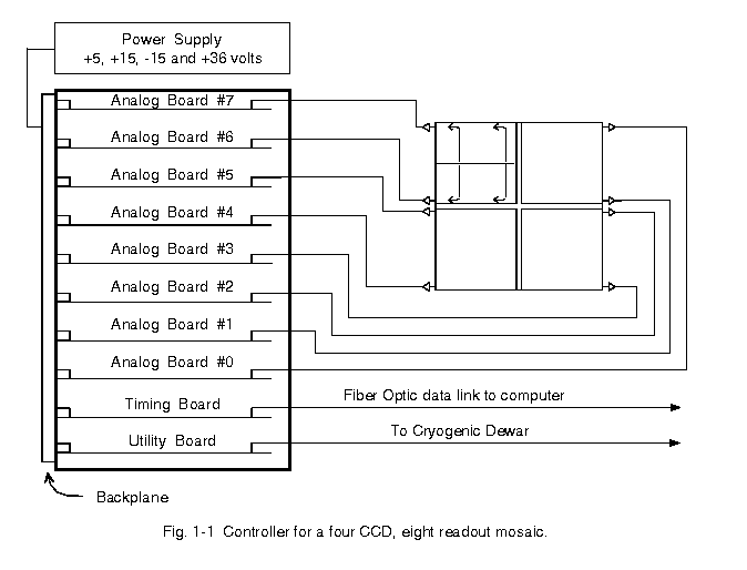
Figure 1-1 shows a schematic of a possible realization of the multiple readout
controller. Systems this complex can be efficiently used with the controller,
but in practice have not been constructed, and are towards the limit of what
is practical with this design. The controller is resident in a chassis with a
backplane, and contains a utility board, a timing board and eight readout boards
to control a four CCD, eight readout mosaic. A local power supply powers the
controller boards.
These controllers are usable for a variety of both optical and infrared
image sensors and have been operated by a number of groups worldwide. Below is a
list of the types of sensors known to be operated by each institution, with
apologies requests for corrections to groups who are listed incorrectly or
incompletely:
Miscellaneous Loral
Jet Propulsion Laboratories
SDSU/Mt Laguna Observatory
Loral 2048 square
Lick Observatory
University of Hawaii
Steward Observatory
Michigan-MIT-Dartmouth Observatory
Canada-France-Hawaii Telescope
Caltech
Tek 2048 square
Keck Observatory
University of Hawaii
Tek 1024 square
Max-Planck Heidelberg
Michigan-MIT-Dartmouth Observatory
Korea Astrophysical Observatory
Canada-France-Hawaii Telescope
NICMOS 2
NICMOS 3
RCA
TI virtual phase
SYSTEM COMPONENTS
A CCD camera system requires many components in addition to the CCD and
controller electronics. These include the cooling system, housing for the
controller electronics. power supplies, host computer and cabling, both electrical
and fiber optic. The controller boards are described individually first, followed
by the controller housing, cryogenic dewar and host computer and related
software.
Timing Board
The heart of the digital timing board is the Motorola DSP56001, a monolithic,
integer digital signal processor with a 24-bit data word. It has a 16-bit address
space, a fast ALU, extensive on-chip peripheral support and a Reduced Instruction
Set Computer (RISC) architecture that executes most instructions in one
clock cycle (100 nanosec in this design). There are separate address spaces for
on-chip program and data memory, a synchronous serial interface, boot logic and
a simple interface to an external data bus. The DSP56001 functions as a timing
generator by writing 24-bit data words from its internal memory to its external
bus every 100 nanosec, whereby circuitry on the timing board decodes the data
word to support three separate timing functions. A delay function simply halts
processor operation for intervals ranging from 50 nanosec to 12.5 microsec in
50 nanosec increments as a convenient way to implement settling delays or to set
the integration time constant of the video processor. The second timing function
consists of digital control lines connected directly to the backplane that are
updated in several different ways by the DSP. The third function is implemented
by writing 16-bit data words to the backplane, from which each analog board
decodes the data word for selectively updating its DACs. Four of these 16 bits,
plus an additional control signal, select one of the 19 analog boards, while
four more bits select which DAC on the board is to be written to with the remaining
8 bits. One of these 32 selections is intercepted by the timing board for
updating the digital control lines that are connected directly to the backplane.
On power-up or reset the DSP program is read in from a boot ROM, which is a single
byte-wide socketed device for easy re-programming external to the controller.
Programming is done on a cross compiler supplied by Motorola in native DS P56001
assembly language. The supplied program consists of initialization code to configure
the DSP in the desired mode, a command processor, testing and diagnostic routines,
routines to read from and write to internal DSP and boot ROM memory over the fiber
optic link, tables containing readout parameters and timing waveforms, and CCD
readout code. Modifications to the code can be done either by re-programming the
ROM or by modifying the DSP contents over the fiber optic link after the ROM program
is booted. The ROM is an erasable electrically programmable part (EEPROM) that can
be reprogrammed from the DSP via the serial link as well, and a security jumper is
implemented to protect against unauthorized intrusion. Rapid, reproducible and
non-intrusive changes to the CCD clocking voltages for optimization of the CCD
device operation can be made while the CCD is operating by exercising the DSP
memory write command. Support for the backp lane is provided by high current drivers
and a careful timing design to ensure reliable operation when many readout boards
are installed. Since the DSP also reads the pixel data from the A/D converters on
each analog board over the backplane, receivers are also included. The DSP then
writes the data to the fast serial transmitter to be received by the host computer.
Both the transmitted and received data word consist of a high start bit followed by
24 data bits, high true, with the most significant bits transmitted first.
Analog Board
The video signal from the CCD's output drain is connected to a load resistor to
make the CCD FET acts as a source follower. The signal is AC coupled to a classical
JPL-designed preamplifier with a low noise dual FET first stage, a dual transistor
for cancelling out the Miller effect in the FETs, and an op amp for gain. A clamp
circuit follows to keep the input signal close to an average of zero volts so the
following amplifiers are well within their optimum operating ranges. Gain selection
of x2 or x4 allows operation at high light levels with some compromise in readout
noise due to finite A/D converter resolution or low light levels with no such
compromise. A polarity switch implemented with a low resistance JFET analog switch
alternates the next amplifier between inverting and non-inverting operation so the
resettable integrator will integrate up on the baseline pedestal immediately after
the CCD is reset, and down on the video signal after charge is coupled onto the
output node of the CCD. This is a classical dual-slope integrator and is the optimum
signal processing algorithm for CCD signals that are dominated by white noise in the
relevant passband. A buffer stage after the integrator allows the zero signal level
of the CCD to be set close to zero digital counts, and is set with a programmable
DAC. This stage drives the 16-bit Crystal Semiconductor A/D converter, which has a
10 microsec combined sample/hold and conversion time. The output from the converter
is in serial form, and is converted to parallel form by two shift registers before being
placed on the backplane for reading by the DSP and transmission over the fast optical
fiber link to the host computer.
Clocking signals for the CCD transfer and reset transistor gate are generated
by a bank of twelve 8-bit DACs that were chosen for their speed and low glitch
energy. They provide a voltage resolution of about 80 millivolts, and an output
over the range of +10 to -10 volts. The DAC output is buffered by a fast op amp
that can drive large capacitive loads. A set of 12-bit DACs generates the DC
bias voltages - seven of them for the CCD and one for the offset adjustment of
the video processor. Three of these voltages are unipolar and four are bipolar.
Twelve bit DACs were chosen to provide greater long-term stability than 8-bit
DACs, but are only settable to 8 bits, as their four least significant bits are
grounded. Long term voltage stability to better than 5 millivolts is achieved.
Additional circuitry on each board provides an interface to the backplane and
decodes the five board select signals (D12-D15, A0), and the four DAC select
signals (D8-D11). One of these 16 codes selects a programming sequence for the
12-bit DC bias supply DACs, which is a two step programming process. Regulators
are place liberally throughout the board to minimize coupled noise and minimize
switching glitches, and are located on the power supply input of every DAC, on
the supply lines to the A/D converter, and on the +/- 12 volt supply lines to
the video processor.
Notice that no potentiometers are used anywhere in the controller, as all
adjustable voltages are set digitally by the DSP. The analog board is implemented
on a six-layer printed circuit card with careful isolation between digital grounds,
the noisy analog and digital ground surrounding the clock drivers and logic
circuitry, and the quiet analog grounds in the video processor. Ground planes
are placed liberally throughout the circuit, and a careful physical placement
of components isolates these circuits as well.
Utility Board
The utility board provides a miscellany of support functions that are not
directly involved with readout of the CCDs. These include, but are not limited
to, exposure timing, CCD temperature control, and system voltage and temperature
monitoring. Based around a DSP56001, it is programmed by SDSU to support these
functions, and can be programmed by the user to support other functions (such
as an additional temperature controller, dewar level and ID, shutter status, LED
driving for status, switch monitoring for direct system control without a host
computer) by programming the use of a number of uncommitted I/O pins. The board
has the same form factor as the timing board, and resides on the backplane.
Communication with the timing board can be either through the asynchronous
serial port of the timing board's DSP, through a 9-pin RS-232 connector on the
utility board, or through two asynchronous serial lines on the backplane.
Power Control Board
The power control board conditions the DC power to protect the CCD from over
voltage transients. The board passes three analog voltages (high voltage,
nominally +36V, and low voltages, nominally +/- 15V) from the power supplies to
the backplane in a controlled manner so that short high voltage spikes are not
passed on to the analog board. The board plugs into the back of the backplane, is
parallel to it, and is six slots wide. It allows the utility board to turn on
switches only after the digital supply has stabilized, all DSPs have had their
software loaded and the DACs on the analog boards have all been set to their
proper values. On command from the utility board the power control board slowly
turns on the +/-15V supplies to the system backplane following a linear ramp of
about 20 milliseconds duration, after which the high voltage is switched on
after the utility board signal.A bank of comparators examines the three analog
supplies and the +5V digital supply to prevent any of the analog supplies from
being switched on to the system backplane if any of them are out of range, and
turning off all analog supplies in the event of a power supply failure after
the power has been turned on. A power-on reset circuit examines the digital
supply and resets the utility board if is is not within range.
VME Interface Board
The VME interface board provides a communication path between the fiber optic
link on the timing board and the host computer. It sends commands from the host
computer to the timing board following the 24-bit protocol of the serial link,
and accepts image data from the timing board and writes them to VME memory using
an on-board DMA (Direct Memory Access) controller. Image size is only limited by
the 32-bit addressing range of the VMEbus, as entire images can be written to
VMEbus memory without intervention from the host processor. This allows non
real-time operating system such as UNIX to be used in the host computer, and
permits concurrent operation of the host computer even during image readout.
Exposures are initiated by the host computer, timed by the utility board, then
placed into memory by the interface board, after which the interface board
signals to the host processor that the image is available in memory so it can be
processed, displayed and stored by the host computer.
The interface board utilizes a DSP56001 processor for housekeeping and DMA
address generation. A local buffer memory (32k x 24 bits) stores incoming image
data to avoid lost data if the VMEbus is unavailable for short periods.
Interrupts can be generated by the interface board, and VMEbus memory can be written
to or read from under control of the on-board DSP. The host computer communicates
with the interface board by writing to a single memory mapped address, and is denied
direct access to the on-board buffer memory.
Backplane and Power Supply
The backplane is simply implemented as a VMEbus J1/P1 backplane whose pins and
timing have been completely redefined for this application. 96-pin DIN connectors
provide a plentiful number of reliable pins, while the multilayer backplane
provides good power distribution and noise suppression. DC power is distributed
to the boards through the backplane, using the +5 connection for +5 volts, whereas
the +/- 12 volt connection is powered with +/- 15 volt supply that is then
down-regulated to +/- 12 volts on each analog board. The high voltage supply,
nominally +36 volts, that is required for operating the drain of the CCD on-chip
amplifier is brought onto the analog boards separately, to insure low noise
operation, and is heavily filtered as well. The boards are all of the standard
VME 3U width, that is, roughly four inches wide, but longer than the VME standard
by about 50%. The number of VMEbus boards used in a particular installation is
determined by the number of analog readout boards that are required; up to 21
connector VME backplanes are available, allowing 19 readouts if a timing and
utility board are installed. It is expected in typical installations that the
backplane and controller boards will be mounted as close as practical to the
CCD, which is typically on the side of the cryogenic dewar containing the CCDs.
Robust grounding of the analog boards at the CCD connector end is required for
low noise operation in multiple readout configurations.
The backplane supports full 24-bit data words on both reading and writing.
While the analog readout board reads 16 of these bits, it writes 16 bits containing
image data and an 8-bit identification tag that is equal to the jumpering of the
address selection jumper block. our address lines, A00-A03, are carried on the
backplane in order to address the A/D converter when transferring pixel image
data to the DSP. This makes the backplane a D24:A04 system. It is not a bus in
the normal sense since only the timing board can be a master, and no bus
arbitration circuitry is needed. A complement of 21 timing signals generated by
the timing board are also carried over the backplane, while only seven of these
are currently used by the analog board. These additional signals could be used
to operate such devices as a programmable CCD temperature controller, a shutter,
diagnostic hardware, filter wheels and so on. Two interrupt input lines to the
DSP are also available on the backplane, which can be used to implement a hardware
timing circuit for overall exposure timing that would be independent of the host
computer.
Controller Housing
The controller boards are housed in a rugged box that is attached to the side
of a cryogenic dewar. It is mounted to the dewar on four standoff spacers, and
contains a hole in the baseplate for passing through a 61-pin hermetically
sealed circular connector attached to the dewar. Short wires run from this
connector to the analog and utility boards, and are totally enclosed by the housing
for electrical isolation from potential external sources of interference. The
housing contains a six slot VME backplane for accommodating a timing board, a
utility board and up to four analog readout boards for implementing quadrant read
out, a power control board, and internally mounted fans. Built of aluminum, it
has a skeleton to which removable panels are attached with screws for easy access
to the controller boards for diagnostic probing. Six panels, all except the bottom
plate that attaches to the dewar, can be removed while the controller is operational.
The box is sealed from the outside so cooling occurs by circulating air inside the
box through the boards, relying on heat conduction to the box. This is done to
minimize dust and dirt contamination of the controller boards and to allow the
boards keep their internally generated heat when operated in cold climates. The
outside housing dimensions are (inches) 13.25 L x 6.75 H x 5.50 W, or (mm) 33.30
L x 16.20 H x 14.0 W.
Cryogenic Dewar
The standard dewar implemented by SDSU is a model ND-5 nitrogen dewar purchased
from IR Labs (IR Labs, 1808 E. 17th Street, Tucson AZ, 602- 622-7074) with additions
for mounting the CCD, wiring to it and controlling its temperature. Liquid nitrogen
tank capacities are available from 1.5 to 3 liters, with the smaller capacity chosen
for operating smaller CCD for less than 24 hour hold times, and the larger capacity
chosen for greater than 24 hour hold times with 2048 square CCDs. The dewar has an
8-inch diameter front plate containing an AR-coated quartz window in front of a
working volume that is six inches in diameter and three inches deep where the CCD
is placed. The CCD is placed in a socket that is attached to a glass epoxy support
structure that attaches to a clamp ring on the inside of the dewar wall, allowing
focal distance, tilt and rotation adjustments with the aid of an alignment jig.
Cooling is transferred from the nitrogen cold plate to the CCD with a cold strap
that is trimmed to bring the CCD close to the desired temperature and then a small
resistive heater actively brings it to the desired temperature under control by the
utility board with a small forward biased diode acting as a temperature sensor.
A calibrated temperature sensor gives absolute calibration of the CCD temperature
to one degree Celsius.
Host computer and control program
Two related host computer architectures have been implemented by SDSU. They are
both built around the SPARC CPU chip set developed by Sun Microsystems, and execute
a program written in-house execute the operating system SUN OS 4.1.3. One
architecture consists of a Sun workstation connected via a host adapter to a
separate VMEbus chassis that memory maps the workstation's S-bus to the VMEbus
memory space. Data is transferred between the buses at a rate of approx. 4 Mbytes/sec.
Commands are written from the workstation to the memory-mapped VMEbus interface board,
and images and replies from the VMEbus interface board are written to VMEbus memory
and then read by the Sun over the host adapter.
The second architecture puts the SPARC chip set on a VMEbus board located on the
same backplane as the interface board to the timing board and the VMEbus memory so
that images can be transferred from VMEbus memory to the Sun over the faster VMEbus.
The computer system is more compact since it is resident in one chassis, and occupies
four VMEbus slots - two for the CPU, and one each for the VMEbus memory and interface
boards.
A program named "ccdtool" executes on the Sun to acquire images and manage the
controller. It is a windowing program written in C with the Xview graphical tools
conforming to the OpenLook graphical user interface. It sets up the three controller
CCDs with either download or on-board application programs, sets user parameters,
issues exposure sequence commands, allows individual manual commands to be issued
and writes images to disk in the FITS format. IRAF is used for image display and
analysis, reading the images from disk.
DSP Software and communications
A typical system will have a total of four processors that need to communicate
with each other - the host computer, the VME interface board, the timing boards
and the utility board. The last three of these have DSP processors. The boards
communicate along a linear path shown in Fig 1-2.
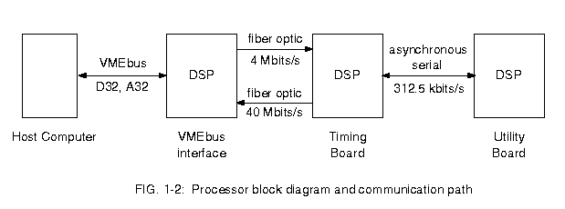
The method of communication between each processor ranges from VMEbus backplane,
to medium speed fiber optic to slow asynchronous serial links. To allow communication
between non-neighbouring boards a communication protocol is implemented in the DSP
program of each of the three boards, and should be followed by the instrument control
program residing in the host computer. The protocol specifies that three types of
data packets exits - commands, replies, and image data. Commands and replies are
multi-word, short strings that are passed between any of the four components of the
system, whereas image data can only be passed from the timing board to the interface
to the host computer. Commands and replies always contain a header identification in
the first word, formatted according to:
Source byte, destination byte, number of words in string.
This is a three byte word, which fits nicely into the 24-bit data word length
of the DSP, and source and destination designations are assigned to each of the
four processors as follows:
0 Host computer
1 VME interface board
2 Timing board
3 Utility board
The number of words in the string can be from two to seven, and count the
header as one. Command strings contain an ASCII three byte, upper case command in
the second words, optionally followed by several numbers whose meaning depends on
the commands. Replies similarly have and ASCII three byte string as the second
word, and typically only contain two words total. For example, the command for
the host computer to write a NOP instruction to the Utility board P: memory in
the $78'th location is:
The utility board will respond to the host computer with a reply:
meaning that the indicated command was executed satisfactorily. The $1
in the most significant nibble of the address field of the WRM instruction is
an encoding scheme to indicate the P: (program memory) is to be updated; X: and Y:
data memory can also be accessed.
A hiearchical philosophy has been adopted in partitioning which boards perform
which time critical tasks. The most time critical tasks of CCD readout timing
and voltage control are performed by the timing board which operates on a time
scale of order one microsecond. Similarly, the VME interface board performs time
critical tasks limited to data handling on a microsecond time scale. The utility
board is next in the hierarchy, performing tasks on a time scale of order one
millisecond. Non-time critical tasks are performed by the host computer.
Parallel to this hierarchy, the microsecond time scale boards are capable of
only limited error checking and reporting and rely on other system components to
manage them. The utility board performs modest error checking and reporting, and
initiates timing and VME interface board operations. Finally, the host computer
performs extensive error checking and reporting on a non-real-time basis, and
directs the utility board to manage time critical operations. As an illustration,
the sequence of commands needed to execute a normal timed and shuttered exposure
is:
| Host writes exposure time to utility | $000304 'WRM' $400018 time
|
| Host writes # of columns to timing | $000204 'WRM' $400001 #cols
|
| Host writes # of rows to timing | $000204 'WRM' $400002 #rows
|
| Host writes number of pixels to VME | $000104 'WRM' $200007 npxls
|
| Host sends start exposure command to Utility | $000302 'SEX'
|
| Utility sends clear CCD to timing | $030202 'CLR'
|
| When done, timing send done clear to utility | $020302 'DON'
|
| Utility opens shutter, starts exposure timer internal utility board operations
|
| When timer elapses, utility closes shutter, sends start readout command to VME interface | $030102 'RDC'
|
| Utility send start readout command to timing | $030202 'RDC'
|
| VME sends done reply to host when readout complete | $010002 'DON'
|
The timing board sends image data to VME interface, which writes it first to
on-board buffer memory then to the VMEbus. When npxls have been sent the timing
board re-enters either idle mode or stop mode depending on whether a 'IDL' or a
'STP' command was last issued, and the VME interface enters command interpreting
mode.
During readout the VME interface interprets all data coming from the timing
board over the fast fiber optic data link as being image data. Both the interface
board and the timing board are still looking for commands to allow the host computer
to abort the readout in progress if needed. Proper management of the readout
parameters is assumed by the host computer, but any task requiring time critical
service is initiated by one of the DSP boards.
An initialization procedure is needed after system reset. Because the procedure
is not time critical and requires a modest degree of checking to insure that it is
completed successfully, it is performed by the host computer:
| Test system: | $000103 'TDL' number | reply: $010002 number
|
| $000203 'TDL' number | reply: $020002 number
|
| $000303 'TDL' number | reply: $030002 number
|
| Load VME program | $000103 'LDA' 2 | reply: $010002 'DON'
|
| Load timing program: | $000203 'LDA' 2 | reply: $020002 'DON'
|
| Load utility program: | $000303 'LDA' 0 | reply: $030002 'DON'
|
| Turn on analog power: | $000302 'PON' | reply: $030002 'DON'
|
The commands will reply with 'DON' after completing command execution about 10
milliseconds later, if successful. Further system checks after this initialization
procedure completes can be made by reading the values of the analog voltages from
the utility board Y: data memory table with the 'RDM' command, and performing
additional 'TDL' tests after full system initialization.
 Back to Document List Page.