
This chapter describes the Sbus interface board that communicates over the fiber optic data link between the timing board and host computer. The board serves the same function as the VMEbus interface described in chapter 6, but has the advantage of plugging directly into Sun workstations. This may be of interest to users of Sun workstations since an intermediate VMEbus chassis, memory and communications link are no longer necessary. The interface board contains a DMA (direct memory access) controller with 24-bit word and address counters that writes image and reply data directly to Sun system memory without processor intervention, enabling large images to be read out without burdening the host processor.
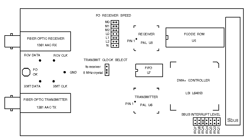
Fig 8-1 shows the layout of the interface board. Three sets of jumpers can be configured to customize the board, but will normally not need to be altered by the user. The set of seven jumper blocks in the top middle controls the frequency range of the fiber optic receiver circuitry by defining a range within which the phase locked loop of the clock recovery chip operates, as follows
| 4 MHz (self-test) | 40 MHz (default) | 50 MHz | ||
|---|---|---|---|---|
| M0 | open | jumper | jumper | |
| M1 | open | jumper | jumper | |
| M2 | jumper | jumper | jumper | |
| L0 | open | open | jumper | |
| L1 | open | jumper | jumper | |
| L2 | jumper | jumper | jumper | |
| N | jumper | open | open |
The default setting is 40 MHz, which is the frequency of the timing board transmitter. The 4 MHz setting is used to exercise the interface board in a loopback self-test that maps the 4 MHz transmitter of the board directly to the receiver. The 50 MHz frequency may be of interest in the future if/when the speed of the timing board serial transmitter is increased. Both transmitter and receiver have been tested at the 50 MHz.
The small jumper block at the center of the board selects the source of the transmitter clock from either a crystal clock or the clock output of the fiber optic clock recovery chip. The second option exists for possible future use to synchronize data transmission with receiving on this board so it is also synchronized on the timing board where it may be advantageous for noise reduction. This may be implemented as a change in the transmitter PAL (programmable array logic) U6 at some time in the future, so in the meantime, the jumper should be left installed in the default configuration which is closest to the clock oscillator.
The final set of jumper blocks selects the interrupt request level (IRQ) when the board requests SBus interrupt service. In the Rev. 3A board there is an error in the labeling of these levels, as they are shown running from level 0 to 6, whereas in reality they are defined in the SBus specification as running from 1 to 7. The default is level 5, which is labeled as IRQ4 on the board. This is fixed in revisions later than 3A.
A commercially available part made by LSI Logic Corp. known as the L64853A enhanced SBus DMA controller, orchestrates communication with the SBus. Generally known as the DMA+ chip, it is implemented in a CMOS gate array process to function as a complete SBus interface, handling all the communications protocol between the interface board and the SBus. It has an internal address counter that is incremented and a byte counter that is decremented each time a byte is written into the internal cache memory of the device. Once 16 bytes are accumulated in the cache the chip requests ownership of the SBus and writes the data out as four longwords, generating the virtual address and writing the data and control signals as required. The DMA+ chip also operates in slave mode to reading and writing to its internal registers and for writing to the board's serial transmitter.
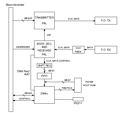
Fig. 8-2 shows a block diagram of the main circuit functions of the interface board. The transmitter PAL accepts 24-bit data D0-D23 from the SBus connector when the parallel load signal PE* is asserted by the address decoder PAL whenever the host computer writes a long word to address 0x400008(PA22=PA3=PA2=1, PA23=PA4=PA1=PA0=0). The transmitter PAL generates clock and data signals at a 4 MHz rate for the fiber optic transmitter chip. Twenty four data bits and one start bit are generated on the rising edge of the clock, most significant bits first. The DMA+ chip asserts the acknowledge signals Ack0-2 to signal to the SBus that the data transfer process has succeeded.
Serial data is received by the fiber optic receiver and sent to a clock recovery chip that generates a clock signal synchronized to the data using a phase locked loop amplifier. The synchronized clock and data signals (RCVCLK and RCVDATA) are buffered by the receiver PAL and sent to a serial-in parallel-out shift register that outputs data a byte at a time to a FIFO (first-in first out) memory. The shift register is cleared at the beginning of each serial word and data is sampled on the rising edge of the clock. The shift register has an internal set of latches, so the PAL generates a signal (LATCH) to latch each byte every eight bits of incoming data, after stripping away the start bit from each data word. Soon after each byte is latched into the shift register it is written to the FIFO. Once a byte is written to the FIFO the empty flat EF* of the FIFO is de-asserted, which connects to the DMA request input line of the DMA+ chip. If DMA operations have been enabled it will assert the DMA acknowledge line which is connected to the read line of the FIFO, causing a byte of data to be written on the data lines and transferred to the DMA+ chip. Once inside the DMA+ chip the data sit in an internal cache until 32 bytes have been accumulated, after which they are written to the SBus as four longwords in a single burst.
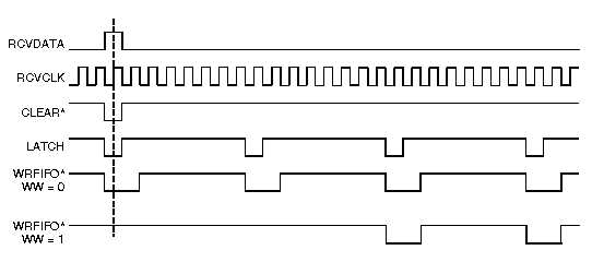
The interface receiver operates in two modes depending on whether it is processing replies to commands or image data. Replies contain 24 bits of significant data so are written as 32-bit data words over the SBus, whereas image data only contain 16 bits of data and are written as 16-bit data words. As shown in Fig. 8-3 below, reply handling is implemented by generating four WRFIFO* pulses for each data word, the first (most significant) one being a zero since it occurs right after the shift register is cleared. For image data only two WRFIFO* pulses are generated per word, on the two least significant bytes of the input data word. Switching between modes is effected by writing a 0 or 1 to the address 0x4xxx1c (PA22=PA3=PA2=1, PA23=PA4= PA1=PA0=0), where the default is WW = 0 (reply mode), as follows -
Command/reply mode 24 bits -> 32 bits WW = 0 (default)
Image data mode 24 bits -> 16 bits WW = 1
The control program keeps track of which mode of data is expected to be transmitted from the timing board and sets the WW bit accordingly.
There is a boot ROM that is accessed by the host computer when the device driver is loaded that contains a unique identifier and some information about the memory allocation. A device driver has been written for SUNOS 4.1.3 and Solaris 2.x that is loaded when the operating system boots to facilitate communication between the user program and the interface board. The boot ROM supplies the board name "SDSUastro" to the device driver as well as the addresses of its internal registers. If a working board is installed, during the boot process the board will be recognized, the ROM will get read, and a message will be displayed
Probing / iommu@0,1000000 ... SDSUastro
Later in the boot process the host computer will attempt to load the device driver and display the message
At TOP of install astro.LOAD, , , ,
astro: SDSUastro0 at SBus slot 1 0x400000 and SBus slot 1 0x800000 and SBus slot
0xc00000 pri7 (sbus level 5)
module loaded; id = 3
The device driver is located in the ftp area in the 'UNIX/' directory, and there is a file named 'astro_install_instructions' that details the installation procedure.
Finally, there is a jumper block for selecting the interrupt level of the board, as discussed above. As the device driver is now written the board will request interrupt service at the end of a complete image transfer and whenever a reply is received, causing the host to execute an interrupt service routine that interacts with the UNIT control and acquisition program. This interrupt level must be the same as what is programmed into the ROM.
 Back to Document List Page.