
This chapter has been updated to describe the circuit board Revision 3B and is dated 1/3/97.
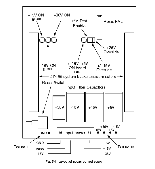
The power control board conditions the DC power to protect the CCD from over voltage transients. The board passes three analog voltages (high voltage, nominally +36V, and low voltages, nominally +/-15V) from the power supplies to the backplane in a controlled manner so that short high voltage spikes are not passed on to the analog board. Fig. 5-1 shows a layout of the principal components of the board. The voltages are input to the 6-pin power connector at the bottom of the board (the mate is an AMP 640585-1 with 350550-1 contacts, supplied with the board), and output to the system backplane through the two DIN 96 pin connectors attached to the board. The board plugs into the back of the backplane, is parallel to it, and is six slots wide.
The +5V digital supply is not controlled by this board, allowing the DSPs on the timing and utility boards to boot before analog power is turned on. After these DSPs boot, the host computer can issue commands to load all DACs to their proper values before analog power is applied. A Power-ON command (PON) is issued to the utility board to begin the power-on sequence in conjunction with the power control board. The first step is to turn on the two low voltage supplies to the system backplane. This is done by the utility board toggling the LVEN line 128 times. Once this is done the two green LEDs will glow, indicating that the two low voltages are available to the system. The turn-on is a slow ramp that takes approximately 20 milliseconds to complete in order to allow analog circuitry in the system to turn on gently without voltage spikes or surges. The next command to be issued by the utility board is the high voltage power-on command HVEN, which also requires 128 toggles. The amber LED turns on once the high voltage is available on the system backplane. The high voltage supply output of the power control board is coupled to the +15 volt supply through a diode, forcing the high voltage output to follow the low voltage output until the high voltage switch is turned on. The most recent revision of this board (3B) has jumpers installed so that the LED's can be disabled for uses where the glow of the LED's may be interferring with data acquisition.
A bank of analog comparators U1 and U2 samples the four incoming voltages to take corrective action if they should go out of range. The jumper +5V test Enable (JP3) can be removed if a sampling of the +5V digital is not desired. If any one of them is out of range all three analog voltages will be turned off, leaving only the +5V digital supply switched onto the system backplane. The table below lists the voltage ranges that are required for the control board to turn power onto the backplane. The voltage ranges are maintained to about a two percent accuracy by resistors R2-R25.
| high voltage | +29.0 to +38.6 | amber LED |
| positive low voltage | +14.8 to +17.8 | left green LED |
| negative low voltage | -14.8 to -17.8 | right green LED |
| digital voltage | +4.75 to +5.25 |
Because power to the analog comparators is derived from the low voltage supplies an additional level of checking is provided by two relays K1 and K2 that switch off if either positive or negative supply voltage is below 11.7V, also turning off the analog supply switches to the backplane. This insures that the comparators have enough supply voltage to give correct readings before the analog supply can be turned onto the backplane. If K1 and K2 turn on then the red LED will glow, indicating that power is available to the control board.
For testing purposes several jumpers can be installed to override the power supply voltage constraints described above. Inserting a jumper on the jumper block +/- 15V Override (JP1) will turn on the two low voltage supplies, and putting one on +36V Override (JP2) will turn on the high voltage analog supply onto the backplane.
A reset circuit is provided on the board to reset the utility board in a reliable fashion. The intention is to override the utility board reset in systems that have a power control board, but to provide a separate utility board reset function for those systems that do not have a power control board. The circuit will reset on +5V digital power-on, when the on-board reset switch is depressed, or when the external reset line connected to pin #5 of the 6-pin AMP power input power connector is grounded. The reset circuit asserts the backplane line UTLRST connected to the utility board after a delay of a few milliseconds to protect against switch bounce.
The 16V8 PAL is provided on the board to coordinate the various voltage control functions. The PAL equation is as follows for the SDSU I:
CLRA = REFPWR' # INPPWR' # UTLRST' # PWRST
CLRB = QA7'
UTLRST = LPENAB & NSWRES
PWROK = REFPWR & INPPWR
CLRA = REFPWR' # INPPWR' # LPENAB' # NSWRES' # PWRST
CLRB = QA7'
PWROK = REFPWR & INPPWR & LPENAB & NSWRES & PWRST'
EXT_T_RST = NSWRES
UTLRST = TIM_U_RST
where # means logical OR, & means logical AND and ' means logical invert. CLRA will be asserted if any of the following four conditions occur: either (1) REFPWR = false, indicating that the low voltage supplies are below 11.7 volts, or (2) INPPWR = false, indicating that the bank of comparators has detected that one of the analog supplies is out of range, or (3) UTLRST = false if the utility board is being reset by the power control board reset circuitry or the digital voltage is out of range (if JP3 is installed), or (4) PWRST = true, indicating that the utility board is resetting the power control board. The high voltage will be turned off (CLRB asserted) and the input counter on HVEN cleared if the low voltage counter on LVEN is ever cleared. This ensures that the high voltage can only be turned on by 128 HVEN cycles issued after the low voltage has been turned on.
Several oscilloscope traces of power turn-on and turn-off waveforms have been obtained for several typical system voltages affected by the power control board. Fig. 5-2 shows the slow ramping turn-on of the two low voltage supplies, +/- 15volt, when AC power is turned on to the system. Note the smooth ramp up behaviour of the voltages, and how closely matched the turn-on times are. These times controlled by resistors R34 (for +15 volts) and R35 ( for -15 volts), and have been selected to give equal turn-on times.
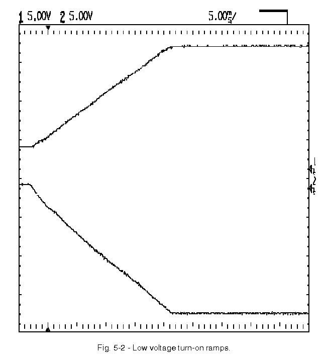
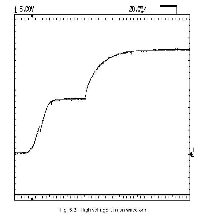
Fig. 5-3 shows the turn-on trace for Vdd, which supplies a drain voltage to the CCD on-chip preamplifier. The first plateau is reached after the two low voltage supplies reach their final values. The second plateau is reached after the high voltage supply is turned on and reaches a stable voltage after all the capacitors and regulators stabilize at 22 volts output.
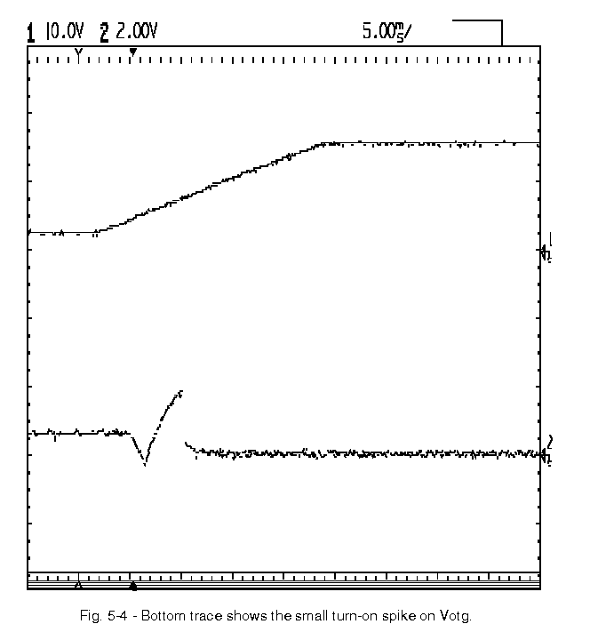
Fig. 5-4 shows the turn on trace for a bipolar DC bias supply output, as measured from pin #4 of the analog board (Votg). The final voltage of the pin is set in software to be zero volts, but there is a turn-on transient of nearly two volts amplitude, with a small negative excursion as well. This output stage is set for a maximum range of -5 to +5 volts, so the voltage is reaching 40% of its maximum range during the transient. This behaviour is typical of the bipolar bias supplies, but is absent from the unipolar ones (analog board pins #1-3) because the high voltage (+36 volts) supply on the driving op amps is not turned on until well after the transients have settled away. The transients are caused by an instability in the Analog Devices 7247 DACs as their power supplies cross 6-7 volts. The shape and amplitude of the turn-on transient is sensitive to the slope of the +/- 15 volts turn on ramps, and particularly to the relative slopes between the +15 and -15 volts supplies. Making the slope equal seems to minimize the transient, but not eliminate it. Furthermore, the transients are affected by the number of analog board plugged into the system, and variability in the particular DACs used on the analog boards. Fig. 5-4 is an atypically large transient obtained with one analog board installed in the system, shown as illustration of the behaviour. The maximum and minimum values of the transient are tested for all delivered power boards, and the values are recorded on the test sheet. For the Loral CCDs used in testing in our laboratory a transient of 2 volts is perfectly safe on the Votg pin, so no precautions are required to further safeguard the CCD, but users should be careful to at least test for transients from the bipolar supplies if there is any potential for damage.
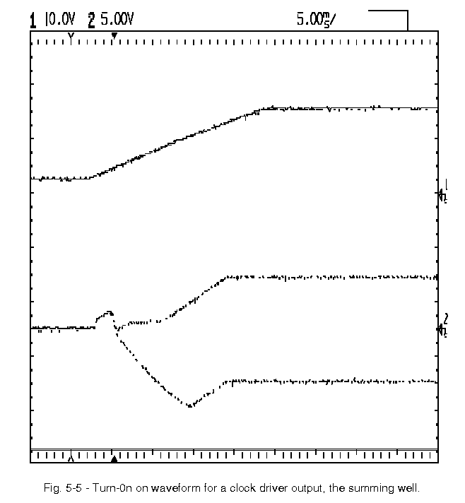
Fig. 5-5 shows the turn-on behaviour of a clock driver, in this case, the summing well clock derived from analog board pin #12. It goes several volts more negative than its normal state during turn-on.
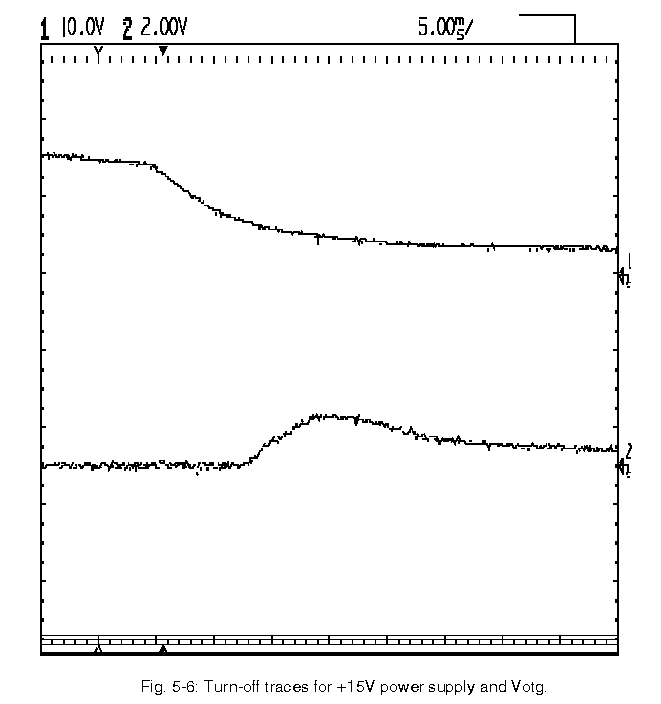
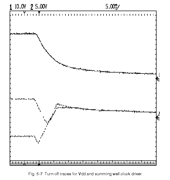
Turn-off behaviour is shown in Figures 5-6 and 5-7. The top trace of Fig. 5-6 shows the turn off of the positive low voltage (+15 volts) as it is rapidly turn off with a front panel knob on the laboratory power supply. The small slope at the beginning of the trace is from this action, and the more rapid fall is caused by the comparator on the power control board sensing that the voltage is below the threshold and turning off the switch to the system backplane. The bottom trace shows the Votg voltage described above, and a small transient similar to the turn-on transient is seen on turn-off as well. Fig. 5-7 (top) shows the Vdd voltage (analog board pin #1) and the clock driver signal from the summing well (analog board pin #12). They both show fairly smooth decay as the power control board switches power off to the analog board.
 Back to Document List Page.