
This document describes the VMEbus interface. There are now two revisions of the circuit board, 2H (a patched derivative of 2E, dated 2/6/92) and 4C (dated 4/5/94). The newer version 4C utilizes a 32 MHz DSP to double the on-board execution speed, incorporates a DSP reset switch and a fiber optic status indicator light, and utilizes PALs that allow some flexibility in the board's architecture. The current version of the DSP software is Rev. 2.30, released May 1994. A constant is defined in the assembler directive to conditionally assemble the appropriate version of the DSP code, since the newer DSP code necessitates several speed related changes.
A block diagram of the VME interface board is shown in Fig. 6-1. A Motorola DSP56001 manages the board functions, channels image and command data and generates VMEbus addresses. The board transmits 24-bit commands and data to the timing board over a fiber optic data link generated from the synchronous serial interface (SSI) in the DSP, and operates at 4 Mbits/sec. A fiber optic serial receiver accepts image data from the timing board at 40 Mbits/sec, de-serializes them with a shift register and stores them temporarily in a latch until a DSP interrupt service routine reads the data into the DSP. Image data is written to the 32k x 24 bit fast SRAM on board, where they accumulate until written over the VMEbus to memory. Socketed EEPROM loads the DSP program into internal DSP program memory when the VMEbus is reset or when the on-board reset switch (Rev. 4C) is depressed.
The interface board is mapped to a single address in the 32-bit address range of the VMEbus, and reads commands written to that address by the host processor on the VMEbus. The address is jumper selectable over the full 32-bit address range, so 31 jumpers need to be set by the user (Rev. 2H) or the address is programmed into PALs A and B (Rev 4C). Address modifiers are set by the DSP code in EEPROM (Rev. 2H) to a24d32 or by PALs (Rev. 4C) to either a24d32 or a32d32. Commands are written as 32-bit words to the interface board, although the most significant byte is ignored by the DSP. The interface board can act as a VMEbus master or slave, and requests bus mastership at the priority request 3 only. Similarly it requests interrupt service at level 5 only, and its responding ID byte is programmable as described below by writing to the on board memory mapped location Y:$FFF4, presently set in the DSP program to $F0.
The DSP56001 has a 24-bit data length and a 16-bit address length. To use the DSP to generate 32-bit addresses for the VMEbus requires a little trickery, as the most significant 17 bits are written to a set of latches with WRHADR only when these address bits change, and the least significant 15 bits are driven directly by the DSP address lines on every write cycle with LADR. Bus ownership can be obtained prior to data transfer operations by an explicit DSP instruction that requests bus ownership, and the bus can be kept until explicitly released, allowing a large number of transfers to occur without the inefficiency of arbitrating for the bus each time. The interface board design can also perform VMEbus reads for transferring images into its memory for post processing, so it can be used as a fast image processor for a limited range of tasks where the DSP's small address space is not an onerous constraint.
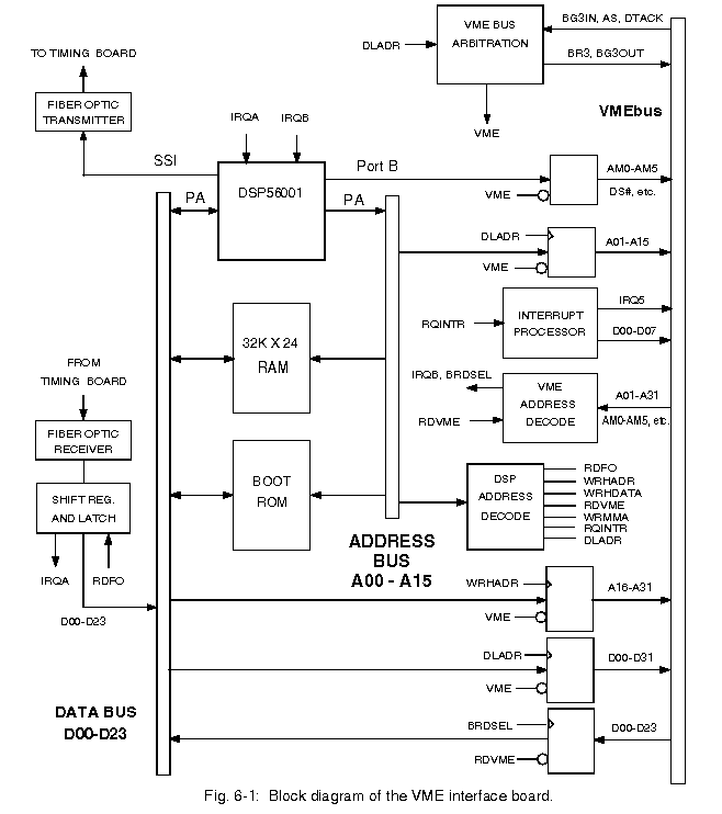
An advantage of using this interface board is that it can fully control the exposure and image acquisition of very large CCD arrays, or even arrays of CCDs. It can write an entire image directly to VMEbus memory without any intervention from the system processor. This frees up the system processor to run any non-real-time operating system (such as UNIX) that is desired, and to be fully dedicated to providing such things as image display and storage, user interface, image processing and so on. Another advantage is that the interface board can place images coming from many CCDs into separate memory spaces on the VMEbus, and can even reorder the pixel data, relieving the system processor of a significant burden.
The operations that can be executed by the interface board are listed below, where A refers to any accumulator or data input register of the DSP, and all operations are described from the point of view of the DSP.
| COMMAND | DSP INSTRUCTION |
|---|---|
| Read input CCD from the serial receiver latch | MOVE Y:($FFF0),A |
| Write data to buffer RAM | MOVE A,X:($4000 to $BFFF) |
| Read data from buffer RAM | MOVE X:($4000 to $BFFF),A |
| Write data to VMEbus | MOVE A,Y:($4000 to $BFFFF) |
| Write data to timing board over serial transmitter | MOVE A,X:($FFFE) |
| Write 16 highest bits of VME address to register | MOVE A,Y:($FFF1) |
| Read data from VMEbus (CONTINUE = 0) | MOVE Y:($4000 to $BFFF),A |
| Read data from VMEbus (CONTINUE = 1) | MOVE Y:($FFF3),A |
| Interrupt VMEbus | MOVE A,Y:($FFF5) |
| Write VME address modifer and interrupt ID codes | MOVE A,Y:($FFF4) |
| Write to Port B of DSP, (X:PBD) | MOVE A,X:($FFE4) |
| Write high data bits D16-D32 | MOVE A,Y:($FFF2) |
| Boot from onboard ROM | same as timing board sequence |
In addition, several functions are directly controlled by Port B of the DSP. They are updated by writing to address X:($FFE4) = X:PBD as listed above, and are defined below. Output means it is asserted by the DSP.
| Output | PB0 | DS0 value asserted on interface board master cycles. |
| Output | PB1 | DS1 value asserted on interface board master cycles. |
| Output | PB2 | LWORD value asserted on interface board master cycles. |
| Output | PB3 | Not used |
| Output | PB4 | AM0 bit asserted during interface board master cycles. |
| Output | PB5 | AM1 bit asserted during interface board master cycles. |
| Output | PB6 | AM2 bit asserted during interface board master cycles. |
| Output | PB7 | AM3 bit asserted during interface board master cycles. |
| Output | PB8 | AM4 bit asserted during interface board master cycles. |
| Output | PB9 | AM5 bit asserted during interface board master cycles. |
| Output | PB10 | REQBUS = 0 to ask for mastership of the VMEbus. |
| Input | PB11 | HASBUS = 1 if the interface is VMEbus master. |
| Output | PB12 | WL = Word Length = 1 if 32 bits, 0 if 16 or 24 bits. |
| Input | PB13 | DONEVME = 1 if VMEbus transfer is done. |
| Output | PB14 | CONTINUE = 1 to continue DSP operation during the VMEbus transfer operation. |
| DSP data word bit | Assignment |
|---|---|
| D00 | AM0 code required to respond to VMEbus writes |
| D01 | AM1 code required to respond to VMEbus writes |
| D02 | AM3 code required to respond to VMEbus writes |
| D03 | AM4 code required to respond to VMEbus writes |
| D04 | AM5 code required to respond to VMEbus writes |
| D05 | LWORD - Long word value of VMEbus address of interface |
| D06 | DS0 - data strobe value of VMEbus address of interface board |
| D07 | DS1 - data strobe value of VMEbus address of interface board |
| D16 | ID00 - bit 0 of ID byte of interrupt generator |
| D17 | ID01 - bit 1 of ID byte of interrupt generator |
| D18 | ID02 - bit 2 of ID byte of interrupt generator |
| D19 | ID03 - bit 3 of ID byte of interrupt generator |
| D20 | ID04 - bit 4 of ID byte of interrupt generator |
| D21 | ID05 - bit 5 of ID byte of interrupt generator |
| D22 | ID06 - bit 6 of ID byte of interrupt generator |
| D23 | ID07 - bit 7 of ID byte of interrupt generator |
Fig 6-2 shows the layout of several banks of jumper blocks and test points. The largest block (Rev. 2H) selects the memory-mapped address in VMEbus space that the board responds to when the host computer writes to it. This address can be selected from the entire 32-bit address space of VMEbus, so requires that thirty-one jumpers either be installed (to select a zero) or not installed (to select a one). The default setting is $00908000, so most of the jumpers are installed. The jumper bank is located right next to J1, the uppermost VMEbus connector. Located next to it is the bank that selects the bit rate of the fast fiber optic data link that receives data from the timing board. Its default setting corresponds to a bit rate of 40 Mbits/sec. Other speeds can be selected by consulting the data sheet for the AT&T 7032PC clock recovery circuit. The address jumpers do not exist on the Rev. 4C board.>
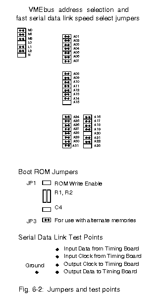
Another block controls the access to the on-board boot EEPROM. The write enable jumper JP1 is installed to allow the DSP to write to the EEPROM. JP3 enables devices other than 8k x 8 devices to be operated; devices up to 32k x 8 can be installed. JP3 is not implemented for Rev. 4C boards, since they only support 32k x 8 devices. The jumper block is located to the left of the bank of four large memory chips above the DSP. The default for Rev. 2.30 DSP software is to have the write enable jumper JP1 not installed but to install JP3 on Rev. 2H boards and to install 32k EEPROMs.
The last part of Fig. 6-2 shows the location of the test points for the serial data link to the timing boards, allowing oscilloscope access to the serial waveforms being passed back and forth to aid in debug. They are located near the optical fiber components.
There is also a jumper JP4 located to the lower left of the DSP on Rev. 2H boards that selects between a 16 MHz clock coming from the VMEbus and an on-board crystal oscillator circuit for driving the DSP.
The jumper should always be installed since the crystal is not installed. A 32 MHz crystal oscillator is installed on Rev. 4C boards to drive the DSP.
The DSP software chapter describes the commands that are located in the "vme boot" program that is loaded from EEPROM after the DSP is reset, and are in common with the other DSP boards in the system. Three application programs have been written for the VME interface board - "vmen" for an arbitrary number of readouts, "vme2" for dual readout, and "vme4" for four readouts. The application "vme1" in earlier versions that would perform single readout to interface with Sun OS device drivers written by Steve Smith of CFHT has been dropped. All applications now write the entire image to VME memory into one memory space for "vme2" and "vme4", or into n memory spaces for "vmen". "vme2" does de-interlacing assuming a single CCD with two amplifiers mounted on opposite corners, "vme4" assumes four amplifiers on a single CCD, one at each corners, and whereas "vmen" does not do any de-interlacing.
As described in the system chapter above, every command to the interface board is prefaced with a header ID word, consisting of a source byte, a destination byte and a number of commands words byte. The interface board is number one, which is determined by firmware. All commands with a one for the destination byte are processed by the interface board; commands with destination bytes of two or three are passed to the timing board through the fiber optic data link, and destination bytes of zero are passed to the host computer through the VMEbus. Headers with destination bytes outside this range are ignored, as processing continues on to the next word in the command string. Replies are made to the VMEbus by writing to an address space specified with the Set Reply Address ('SRA') command, which is of the form
| $000104 | 'SRA' | high 16-bits of address | low 16-bits of address |
Replies to commands will always consist of a header containing source, destination and command length bytes, followed by at least one word that may contain data or ASCII codes. The SRA command will generate a reply to the VMEbus starting at the address specified in its argument list, and the next command reply will start eight bytes away. The reply to many commands is a simple ASCII 'DON' meaning that the command was executed successfully, or an 'ERR' meaning that it was not successful. The replies will be written starting at the VMEbus address indicated by SRA and incremented over a 128 byte range, after which it will restart at the address specified by SRA. Users may either use this circular addressing scheme or may issue frequent SRA commands to keep the address from circling. An addressing limitation is that the 128 byte reply area must not cross a 64k byte VMEbus address boundary. All replies also result in an optional interrupt being requested by the interface board so the device driver can efficiently process the replies. A timeout feature has been changed in Rev. 2.30 to write a 'TIM' reply if a complete command is not received in 50 milliseconds, controlled by the TIMEOUT constant.
Four commands are the same as the timing and utility boards - LDA, RDM, RST, TDL, and WRM. The RDC and ABR commands are also interpreted by the timing board, but execute differently. The additional interface board commands are as follows:
| SRA | high low Set Reply Address - Specify the starting address for all replies to the VMEbus. |
| RDC | Read CCD - Set up interface board to read out CCD. All further data from the timing or utility boards will be interpreted as 16-bit/pixel image data. |
| ABR | Abort Readout, and place interface board in command processing mode. Issue an abort readout command to the timing board. |
| IRQ | Generate an interrupt request. After a waiting period of one second a message of $010002 'IRQ' is sent to the host processor to signal that an interrupt request command has been processed, after which the interface board will request interrupt service at a priority level of 5, with an interrupt vector of $F0. |
SRA is a boot command, and the remaining ones are application commands. A single word is encoded to contain status information about the board processing state. It is located at the data memory word X:0, which can be read or written from the host with RDM or WRM command.
| Host computer command: | $000103 | 'RDM' | $200000 |
| Interface board reply: | $010002 | value |
The following bits are defined for X:STATUS = X:0 -
| bit 0: | Set by the DSP program if it is in readout mode, cleared if in command processing mode. |
| bit 2: | Set if an SRA command has been executed since the last DSP boot. If not then replies will not be generated. |
| bit 3: | Set if a command being processed was received from the timing board, cleared if it came from the host computer. This is used internally for command processing. |
An options word defined at X:1 is used to set firmware execution options. It can be written to or read with the commands:
| Host computer command: | $000104 | 'WRM' | $200001 | value |
| Host computer command: | $000103 | 'RDM' | $200001 | |
| Interface board reply: | $010002 | value |
The following bits are defined for X:OPTIONS = X:1 -
| bit 1: | Set to require that the interface board request VMEbus interrupt service after each command reply and after the all the images have all been transferred. Default is no interrupts. |
| bit 2: | Set to require that the DSP translate the incoming 16-bit straight binary image data to twos complement format for compatibility with the FITS. It will convert data over the range from [0 to 64k] -> [-32k to +32k]. Default is no conversion. |
The DSP code changes in going from 2H to the faster 4C board version are all contained in the "vmeboot.asm" file and are listed below. The first change makes sure the SSI transmits at 4 Mbits/sec so the timing board can still receive its commands.
IF  REV4C
   MOVEP   #$6001,X:CRA   ; SSI: No prescaling, 24 bits/word, on-
ELSE		          ; for a clock rate of 4 MHz.
   MOVEP   #$6000,X:CRA   ; Don't divide by two for the slow board
ENDIF
The second change makes sure that access to on-board EEPROM memory for program access will still meet the access time of the EEPROMs, so twice as many wait states are required for the faster board.
IF  REV4C
   MOVEP   #$0040,X:BCR	  ; Wait states for external memory accesses
ELSE
   MOVEP   #$0020,X:BCR	  ; Wait half as many clock cycles
ENDIF
Finally, the VME board must not transmit the commands too quickly to the timing board or its DSP delay function will miss the second and later command words since interrupts cannot be processed during this time.
IF  REV4C
   COM_DLY  DC	880	  ; Delay for timing board to exit REP instr.
ELSE
   COM_DLY  DC	440	  ; Delay half as much for a slower board
ENDIF
Additionally, a bug that existed in Rev. 2.25 an earlier has been eliminated from Rev. 2.30 - the X:BCR register was cleared, making for fast accesses to on-board EEPROM. Even though the EEPROM still seemed to work when its access time spec was violated on the slower boards, it always failed for the faster boards.
The following changes were made to the file "vmeboot.asm" in making the transition from Rev. 2.25 to 2.30:
(1) The OVERLAY area was put right after the boot code, not at the top of DSP memory. The application code starting address APL_ADR was tuned to optimum. All the application codes were changed to suit.
(2) Timeout code for complete command reception was changed - the timeout period was increased from 1 to 50 millisec, and a 'TIM' reply is now generated so commands can be regenerated by the host computer if needed.
(3) Introduce changes to operate the Rev 4C board which is the new x2 faster DSP circuit. Three changes are needed in the boot code to operate faster and are marked with a "Rev 4C change" in the comment field. A fourth change is needed in both versions.
(a) Insert an extra NOP into the XMT_DLY loop so the same time interval is inserted in between words to the timing board.
(b) Divide the SSI speed by 2 so it still goes out at 4 MHz.
(c) Require 4 wait states for PROM access.
(d) Don't go clearing the BCR register.
(4) Introduce the assembly command line variable REV4C to address revision level dependencies. The file vmeboot.asm - contains code for both the slow (2E) and fast (4C) revision levels of the VME interface board.
This application reads from one to sixteen readouts, placing each one in its own separate memory space in the order in which they are received by the interface board. It is the simplest of the applications, and is suitable for reading one CCD. It can be downloaded from the host computer or loaded from on-board EEPROM memory with the command 'LDA 1'. The program determines which datum goes in which address space strictly based on the order in which the data was received - the first pixel datum goes to the beginning of the first address space, the second pixel to the beginning of the second address space, and so on. The "vmen" program will fill each image space starting at the first address of that space, meaning that de-interlacing of systems containing more than one readout per CCD is not done. The incoming pixel data are first written by an interrupt service routine to the on-board SRAM buffer memory that is set up as a circular buffer of modularity Y:BUF_SIZ = Y:3 = 4096. The starting VMEbus addresses where the image data will be written to are set by the host computer by writing to a table in DSP memory. This table is not overwritten by the DSP program, so only needs to be written only once. The table begins at Y:VME_TBL = Y:$40 and contains pairs of addresses, each pair containing the high and low 16-bits of the 32-bit VMEbus address. A shadow buffer is maintained by the DSP starting at address Y:$60 that contains the current addresses being written to by the DSP, and is initialized to the starting address table at the beginning of readout. For two readouts -
| $000104 | 'WRM' | $400040 | highest 16-bits of VMEbus address, first readout |
| $000104 | 'WRM' | $400041 | lowest 16-bits of VMEbus address |
| $000104 | 'WRM' | $400042 | highest 16-bits of VMEbus address, second readout |
| $000104 | 'WRM' | $400043 | lowest 16-bits of VMEbus address |
Two additional parameters need to be set for a readout, Y:NCCDS = Y:0 and Y:NPXLS = Y:1 -
| $000104 | 'WRM' | $400000 | NCCDS - Number of readouts |
| $000104 | 'WRM' | $400001 | NPXLS - Total number of pixels to be read |
The image data will get written back to the VMEbus at 16 bits per pixel, setting the VMEbus control lines DS0 = DS1 = 0 and LWORD = 1. Once the address table, number of CCDs and total number of pixels are set up readout will begin once the interface board receives an RDC command from any source. The interface board will be placed in readout mode whereby any data received from the timing board over the fast fiber optic data link will be interpreted as image data until the desired number of pixels is received or an 'abort readout' = ABR command is received from the host computer. The number of pixels received since the start of readout can be read from the location Y:IPXLS = Y:2, as follows:
| $000104 | 'RDM' | $400002 | IPXLS - Number of pixels read so far |
The transfer rate was measured to be 580 nanosec per pixel for this firmware, which is a transfer rate of 3.5 Mbytes/sec. For a single readout of 23 microsec/pixel this corresponds to a VMEbus utilization of 2.5% during readout. The utilization can be decreased by a factor of two by programming the 32-bit transfer mode, and will increase in systems with more than readout.
These application programs are loaded from EEPROM with the command "LDA 2" (for "vme2") or "LDA 3" (for "vme4"). Each program will write entire images directly to VMEbus in one single address space, properly de-interlacing the pixels as they arrive so the two or four image sections are joined correctly. The starting VMEbus addresses where the image data will be written to are set by the host computer by writing to a table of in DSP memory. For dual readout the starting and ending address of the image space needs to be written as follows:
| $000104 | 'WRM' | $400040 | highest 16-bits of VMEbus address, starting address |
| $000104 | 'WRM' | $400041 | lowest 16-bits of VMEbus address |
| $000104 | 'WRM' | $400042 | highest 16-bits of VMEbus address, ending address |
| $000104 | 'WRM' | $400043 | lowest 16-bits of VMEbus address |
Four quadrant readout is a bit easier, as only the starting address needs to be specified. The DSP program calculates the three remaining addresses based on the image size. "vme2" is a bit lazy in this respect. These addresses are specified by the host computer with WRM commands, and need only be done once after booting up the board, not before each readout. A shadow buffer is maintained by the DSP starting at address Y:$60 that contains the current addresses being written to by the DSP, and is initialized to the starting address table at the beginning of readout.
One additional parameters need to be set for a readout, Y:NPXLS = Y:1. This variable is defined differently for the "vme2" and "vme4" applications than for "vmen", since it refers here to the number of pixels per readout, not the total number of pixels to be read. NCCDS should not be set for "vme2" or "vme4" since wrongly setting them would really mess things up.
| $000104 | 'WRM' | $400001 | NPXLS - Number of pixels to be read by each readout |
The "vme2" and "vme4" programs do full de-interlacing in real time. For dual readout the first pixel received goes at the beginning of the first address space, and the second pixel goes at the end of the address space. The third pixel goes at the beginning address + 2, and the fourth pixel goes at the last address - 2. Quadrant readout is similar, but increments and decrements by the number of pixels per line also occur at column boundaries. For quadrant readout the number of columns must be specified as:
| $000104 | 'WRM' | $400005 | NCOLS - Number of columns for each readout |
| $000104 | 'WRM' | $400006 | NROWS - Number of rows for each readout |
| $000104 | 'WRM' | $400007 | OFFSET - Number of bias columns to skip |
The OFFSET parameter is introduced so the overscan pixels that normally occur at the end of a readout line will not be placed there but will instead be placed at the beginning of each line. The effect is to put the four bias strips on the left and right hand sides of the image and not at the center so field identification will be easier. The OFFSET parameter should be set to the number of columns minus the number of prescan pixels on the CCD. The order of readout of the pixels should be - lower left had corner, lower right hand corner, upper left hand corner, and upper right hand corner.
At the end of readout a 'DON' reply will be sent to the host computer. The utility board also sends a 'DON' reply after it has completed starting the exposure, so the host computer will receive two 'DON' messages in response to a single start exposure command issued by the host computer to the utility board, one as the exposure begins and one after readout is complete.
KNOWN BUGS: Caution should be exercised if VME boards with master capability are placed in slots after the interface board, if they will be requesting bus ownership simultaneously with the interface board. The prudent thing to do at this time is to place the interface board as the last board in the bus if possible.
 Back to Document List Page.