
The board was developed in the winter and spring of 1995 and first shipped in May of that year. It is board revision 1C and contains no firmware.
This chapter describes the dual readout board that processes the video output from two CCD readouts, and generates DC bias voltages for them. The board contains circuits similar to the single readout analog board discussed in chapter 3, but includes two video processors per board. Systems with four readouts and above can realize significant savings in board space if the CCD readouts are driven in parallel. The clock drivers are not included in this board, so a single readout analog board is required to operate a CCD. Dual readout systems need a single readout analog board for its clock drivers and may utilize this dual readout board for the second readout, though there is no particular benefit to this over using two single readout boards.
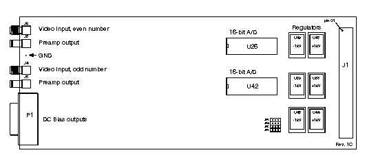
Fig 9-1 shows the layout of the board, and is quite similar to the layout of the single readout analog board. A pair of threaded SMA connector accepts the video (output source) signal from the CCD while a pair of SMB connector (push-on) outputs the video after its been amplified by the preamplifier as a debugging tool. A test point for ground connections is placed in between the two sets of connectors. Two 16-bit A/Ds are provided for simultaneous conversion, and a bank of regulators provides +/- 12V to the board. Below the video connectors is a DB15 MH connector that outputs the DC bias voltages for operating two readouts. Six settable voltages are provided, and labeled OD (output drain), RD (reset drain) and OTG (output transfer gate). Additionally +/- 12V is provided on the connector for powering in-dewar circuitry.
The address of the board is set by the set of four jumpers JP1 to JP4. When the DSP executes a read instruction to read the A/D counts the addresses A01, A02, A03 and X/Y* are compared to the jumper settings. The least significant line A00 is not sampled by the jumper block but by a comparator that selects either the top A/D (A00 = 0, even addresses) or the bottom A/D (A00 = 1, odd addresses). Thirty-two A/Ds can be read from addresses X:$FFB0 to X:$FFBF and Y:$FFB0 to Y:$FFBF. When the DSP executes a write instruction to update the DC bias DACs the data lines D13, D14, D15 and the address line A00 are sampled by the jumper block. The data line D12 is not sampled by the jumper block, but must be a zero to write update the DC bias supplies for either readout.
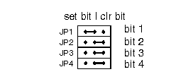
Fig. 9-2 shows an enlargement of the address select jumper block. Jumpers on the left side select the indicated address bit when it is a one, and jumper on the right side selects it if its a zero. This is the reverse of the sense on the single readout board. In the figure the address is a 2, so the top A/D would be selected at a read address of X:$FFB2, the bottom A/D at a read address of X:$FFB3; the DC bias DACs would be written to by selecting the data lines D13-D15 at the address X:$FFB0 with an instruction such as MOVE #$xx2xxx,X:($FFB0). The exact sequence of instructions for updating the DACs is contained in the waveform tables for the 'SBV' (Set Bias Voltages) instruction executed by the timing board located in application programs such as tim1.asm and tim2.asm. The addresses are given below in the table.
The table summarizes the operation of the DC bias supplies. The two offset signals set the output offset level of the video processors. The remaining voltages are available at the DB-15 connector P1 below the video connectors. The wavecode entries are digital addressing designators used by Richard Stover's wavegen program, and is just the complement of the DSP entry listed in the table that actually gets written to the dual readout board to uniquely select one of the DAC registers for updating. The DSP code entries give the two lines of DSP code needed to update a DAC, where the first line updates the data latch U22 with the voltage value and the second instruction selects which DAC to update by toggling one of the bits of the latch U23. The voltage ranges available at P1 is determined by the strapping of the DAC (either +/- 5V or 0-10V outputs) and the selection of gain resistors on the quad op amps U13 and U15.
| P1 Pin # | Signal Name | Wavecode Entry | DSP entry | DSP code | Voltage Range | ||||||||||||||||||||||||||||||||||||||||||
|---|---|---|---|---|---|---|---|---|---|---|---|---|---|---|---|---|---|---|---|---|---|---|---|---|---|---|---|---|---|---|---|---|---|---|---|---|---|---|---|---|---|---|---|---|---|---|---|
| | $002d7f $042cfe | -5 to +5V
| | | | | | | | | | | | | | | | |
Sample DSP code is given here for reading out from the dual readout board. The two A/Ds at addresses 2 and 3 are alternately read by the DSP, and their the data values are written to the fiber optic transmitter.
; Read pixel datum from the A/D and send it along the serial transmitter MOVE Y:CCDSEL2,R0 ; Address of all CCD clocks NOP MOVE X:(R0),A ; Get the A/D converter counts from #0 A/D MOVE A,Y:(R7) ; Send them to the serial transmitter JSR CCDSEL2,R0 ; Address of all CCD clocks XMT_DLY ; Delay for the fiber optic transmitter MOVE Y:CCDSEL3,R0 ; Address of all CCD clocks NOP MOVE X:(R0),A ; Get the second CCD datum MOVE A,Y:(R7) ; Delay for the fiber optic transmitter to work XMT_DLY REP Y:CCDSEL2,R0 ; Address of all CCD clocks FO_DLY NOP RTS ; Define addresses of A/Ds on dual readout board CCDSEL2 DC $FFB2 ; Address of dual readout board's first A/D CCDSEL3 DC $FFB3 ; Address of dual readout board's second A/D ; This definitions depends on the revision level of the VME interface board IF REV4C FO_DLY DC 6 ; Delay for timing board to exit REP instr. ELSE FO_DLY DC 12 ; Delay a little more for the slower
 Back to Document List Page.