
The analog board is described in this chapter, and includes sections on hardware preparation, theory of operation, timing and board construction. It describes the current revision Rev. 4B of the board.
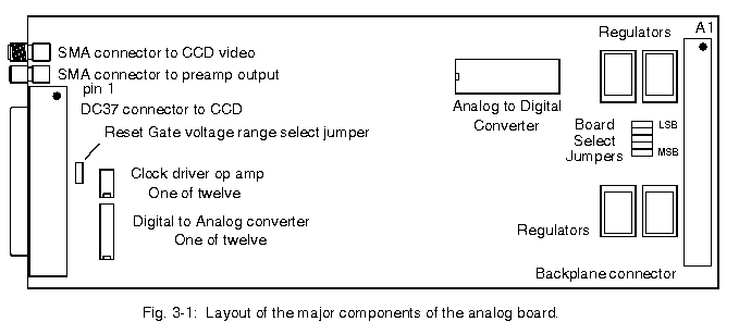
Figure 3-1 shows the layout of the principal components of the analog board. The DC37 connector on the left hand side connects the clock driver, DC bias and grounds to the CCD, and can be used to supply filtered +/-12 volts for powering preamplifiers next to the CCD. The CCD video is carried from the CCD on a separate shielded coax to the top (threaded) SMA connector, from which it is amplified and filtered by video processing circuitry before being converted by the A/D converter before transmission over the backplane connector and backplane to the timing board for eventual transmission to the host computer over the fiber optic link. The SMA connector below it is a test output from the output of the preamp stage, which is a good place to connect an oscilloscope for monitoring CCD waveforms. Each one of twelve clock drivers contains a digital to analog converter and an op amp, one of which is shown on the left hand side of the figure. Four high current regulators mounted on heat sinks condition the power from the backplane, and numerous small current regulators distributed throughout the board provide further local regulation.
Two sets of jumpers need to be set by the user. The first is the board address select, determined by the jumper blocks near the backplane connector. Addresses from 0 to 31 are allowed (except 15, which is used for functions on the timing board), and 0 to 14 should be used first for simplicity of the readout software. Five jumpers must be place in the jumper block - jumpers placed nearest the backplane connector will select a zero, and jumpers placed on the other side will select a one. Fig. 3-2 illustrates this.
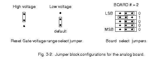
Provision is provided for selecting the voltage that drives the op amp of the circuit providing the reset gate clock signal to the CCD to allow compatibility with CCDs that require large voltages on the high going pulse, such as the TI 800x800 devices. Placing the jumper towards the bottom of the board selects the default voltage range of -10 to +10 volts for the output of this stage, whereas placing it towards the top of the board selects the unregulated +15 voltage to feed the upper rail of the op amp. If this input voltage is set to +16 or 17 volts then a high enough voltage will be provided for resetting the TI devices, and the correct voltage will be supplied to the rest of the board, albeit at a higher overall power consumption to the board.
The board contains five groups of functions - a set of twelve CCD clock drivers, a set of seven low noise DC bias supplies, backplane interface circuitry, a video processor, and an analog-to-digital (A/D) converter. It is designed as a companion board to the timing board described above, and communicates with it over the backplane. Each function will be discussed in turn below. Part numbers refer to the circuit schematic, which is supplied to users along with the analog board.
Each clock driver can be independently updated on a write cycle from the timing board. For simplicity in this discussion we will refer to the schematic of a single one of these circuits, say the RG driver nearest the output connector J2. It consists of a fast digital-to-analog converter (DAC, U3), an op amp U2, a three terminal regulator (U1) for generating the +5 volts required for unipolar operation of the DAC, level shifting components and various filtering components for noise immunity and wave shaping. An eight bit digital bus updates the latch internal to the DAC whenever its latch enable (LE) line is asserted, which occurs when the appropriate digital code on D08-D11 is generated by the timing board. The DAC output is sent to the inverting input of the op amp U1, where a negative voltage VE- produces a level shift to create a bipolar output of -10 to +10 volts from the unipolar DAC output of 0 to +5 volts. The user may choose other values of R14 to R16 to obtain different output voltage ranges, remembering that the output impedance of the DAC of about 200 ohms adds to R14 for a total node impedance of 1k due to the DAC input. VE+ and VE- are the rail voltages, and are nominally +12 and -12 volts, though this may be adjusted as well by choosing other regulators (U66 and U69). Notice that because U2 is an inverter, the clock driver voltage varies inversely with the digital voltage codes D00-D07 written by the timing board. The voltage change for a change of one count in the digital code is nominally 0.078 volts with the default resistor settings. Due to component tolerances, chiefly in the +5 volts regulators, there is some variability in the output voltage from one clock drivers to the next. This was measured to be 0.15 volts rms, corresponding to 2 counts in the digital voltage code, indicating that some adjustment of the digital voltage code for each clock driver is needed to attain the full accuracy possible with this clock driver circuit. In practice such a small variation in clock driver voltage may not significantly affect CCD operation.
The capacitor C14 is provided for slowing down the clock driver waveform. Since the CCD is a highly capacitive load, the op amp will exhibit a loss of control when it is controlled not by its feedback current but by its current driving capacity. A judicious choice of C14, in the range of 5-50 pf depending on the capacitance of the line, can keep the op amp under control, while also damping out over- and under- shooting. These capacitors are not normally installed on the boards. The filter R18 and C17 is inserted to reduce the rather high noise that the +5 volt regulator U1 produces, since it couples nearly directly through the DAC and shows up on the clock driver output. While the noise couples into the CCD video signal with a coupling constant in the range of only one part in 300-1000, prudence dictates that this filtering be installed. Further power supply decoupling is provided by C13, C15 and C16 to minimize high frequency noise coupling.
A special jumper is provided on the RG (reset gate) driving circuit. It allows a choice of the upper rail voltage for the op amp to allow higher reset gate voltages than the +10 volt nominal, to allow the operation of devices such as the older TI 800x800s. The default jumpering selects the lower VE+ voltage, whereas the higher VS+ voltage can be chosen for those applications. While the noise on the VS+ supply is higher than on the VE+ supply, noise during the reset gate high is only weakly coupled to the video output.
The output connector J2 is labeled with the CCD clock signals according to the names that are assigned in the ROM software that is supplied with the timing board. This is the default configuration to simplify initial setup of the system, and can be freely changed by the user at will by reprogramming the DSP readout program. The output connector J2 that runs to the CCD is defined as follows:
| Signal Name | Digital code | Pin # | Voltage Range |
|---|---|---|---|
| OS = video | none | SMA connector | |
| OD | 2, $C | 1 | 0 to +30 VDC |
| RD | 4, $C | 2 | 0 to +20 VDC |
| available | 8, $C | 3 | 0 to +20 VDC |
| OG | $10, $C | 4 | -5 to +5 VDC |
| available | $20, $C | 5 | -10 to +10 VDC |
| available | $40, $C | 6 | -10 to +10 VDC |
| available | $80, $C | 7 | -10 to +10 VDC |
| RG | 0 | 8 | -10 to +10 V clocked |
| S1 | 1 | 9 | -10 to +10 V clocked |
| S2 | 2 | 10 | -10 to +10 V clocked |
| S3 | 3 | 11 | -10 to +10 V clocked |
| SW | 4 | 12 | -10 to +10 V clocked |
| P1 | 5 | 13 | -10 to +10 V clocked |
| P2 | 6 | 14 | -10 to +10 V clocked |
| P3 | 7 | 15 | -10 to +10 V clocked |
| TG | 8 | 16 | -10 to +10 V clocked |
| available | 9 | 17 | -10 to +10 V clocked |
| available | 10 | 18 | -10 to +10 V clocked |
| available | 11 | 19 | -10 to +10 V clocked |
| +12 VDC | none | 20 | +12 volt power for dewar |
| -12 VDC | none | 21 | -12 volt power for dewar |
| GND | 22-37 | analog ground |
The definitions of the DC bias signals OD, RD and OG are set by the DSP software in the supplied DSP source code, and can easily be redefined by altering that source code. OS = video is on a separate SMA connector, and cannot be redefined; it is the only analog signal input to this board. The connector for the clock and bias signals on the analog board is a DC37 type, part number 17-DC37P-C, and contains male type pins. A suitable mate needs to be provided by the user to connect to the CCD dewar. This DC37 connector is similar in style, but larger than, the popular DB25 connectors used for RS-232 serial connections in computer systems.
A total of seven programmable DC voltage sources are provided on the analog board. One of these has a unipolar range of 0 to +30 volts, and is intended to drive the Output Drain (OD) of the on-chip preamplifier of the CCD. Two more are provided with a range of 0 to +20 volts, one of which is intended to drive the Reset Drain (RD) of the on-chip reset transistor. One bipolar supplies a constricted range of -5 to +5 volts to drive the Output Transfer Gate (OTG) that lies between the Summing Well (SW) and the output node. Three more bipolar supplies range from -10 to +10 volts, and are not assigned in the default configuration. Filters (1k, 1 microfarad) are provided at the output of each supply to minimize noise feedthrough, an important consideration since noise on the drain supplies couples with a coefficient is 0.3 in devices we've tested. Additional filtering is provided on the feedback of each op amp generating the DC voltages. The inputs to the op amps come from a series of four dual twelve-bit DACs, whose four least significant bits are grounded, allowing only the most significant 8 bits to be updated by the timing board. The U24 outputs A and B are both wired for unipolar operation by grounding the ROFS A and B inputs, whereas U37 has one bipolar output (A) and one unipolar output. U25 and U38 have all their outputs selected to be bipolar for eventually driving the DC bias supplies over the range -10 to +10 volts.
The code for updating the OD (Output Drain) DAC is shown. Analog board #3 is assumed, and OD will be set to a voltage of 22.5 volts:
| MOVE | #$ffB0,R5 | Set the address for updating CCD clocks |
| MOVE | #$003CFF,X:(R5) | Set all chip select lines high |
| MOVE | #$003DC0,X:(R5) | Place data on DAC data bus |
| MOVE | #$043CFD,X:(R5) | Hold desired DAC chip select line low for 300 nanosec |
| MOVE | #$003CFF,X:(R5) | Set all chip select lines high again. |
In the supplied DSP code this is written in a more compact form. The values to be written to the X:(R5) memory location are stored in a table of Y: memory and accessed by a single program instruction that simultaneously writes the current table entry to the analog board and fetches the next table entry into an accumulator for writing on the next instruction cycle. This technique is used for updating all CCD clocks as well, and has the benefit that CCD timing and voltage data is not encoded into the readout program but is contained in a Y: memory data table where it is more easily modified and maintained.
The actual 8-bit value to be written to each DAC depends on the voltage range assigned to that function. The table below lists the properties of each of the seven bias supplies, plus the video processor output offset adjustment discussed below.
| Name | Function | J2 pin # | Voltage range | Selection code |
|---|---|---|---|---|
| VP OO | Output Offset | SMA conn. | -5 to +5 | $FE |
| OD | Output Drain | 1 | 0 TO +26.7 | $FD |
| RD | Reset Drain | 2 | 0 to +18.6 | $FB |
| none | not assigned | 3 | 0 to +18.6 | $F7 |
| OTG | Output Transfer Gate | 4 | -5 to +5 | $EF |
| none | not assigned | 5 | -10 to +10 | $DF |
| none | not assigned | 6 | -10 to +10 | $BF |
| none | not assigned | 7 | -10 to +10 | $7F |
There is no inversion of the digital code, so larger codes will give more positive output voltages. The actual voltage ranges for the default component selection is shown in the table above, although on the schematics the OD range is referred to as a nominal 0 to +30 volts range for simplicity. Other voltage ranges may easily be chosen with safety and power consumption considerations in mind by selecting other values of feedback resistors or regulators.
The backplane interface accepts write requests from the timing board to update any one of the clock driver or DC bias supply DACs. U59 is an 8-bit comparator that selects this board for writing to the DACs if the jumpered value of D12-D15 is selected with the correct value of the least significant address bit, allowing a total of 32 analog boards to be installed in the system. In practice this is limited to more like 18 or 19 boards because of the finite length of VME backplanes that are used for inter-board communication. The jumpers JP 2-6 are placed to identify each analog board, and must be uniquely assigned. Jumpers installed closest to the backplane select a bit code of zero; all zeroes is the code for single analog board systems. Once the comparator U59 selects the board for a write operation the decoder ships U56 and U57 select one of the twelve clock driver DACs to update or one of the two latches U51 or U52 to write to for updating a selected DC bias DAC. U51 contains the 8-bit digital code to be written to the DAC selected by the low bit 0-7 that is written to U52, following the DSP code given above.
Read operations over the backplane are initiated by a read from the timing board from one of the sixteen addresses determined by A00 to A03. An additional sixteen analog boards may be read by selecting a read from X: memory space rather than the default Y: memory space. The 8-bit comparator chip U63 generates an output enable signal if the addresses are as indicated by the same five jumpers used for write operations, and causes the 16-bit pixel data contained in the two shift register U62 and U64 to be asserted onto the backplane. The value of the jumpers JP 2-6 is also asserted onto D16-D20 (with D21-D23 grounded) to help the host computer keep track of which analog board originated each image datum. The shift register U62 and U64 are needed because the A/D converter only has a serial word output, and it is too slow to be written directly onto the fiber optic link that goes to the host computer.
A block diagram of the video processor and A/D converter is shown in Fig. 3-3. The video processor consists of a preamplifier that can be connected directly to the Output Source (OS) of the on-chip amplifier of a CCD, a DC restoration circuit, a switchable inverting/non-inverting differential amplifier, a resettable integrator, and a combined driver and level shifter.
The preamplifier is the classic Janesick/JPL dual FET input design. Q1 provides a high impedance, low noise input, while Q2 eliminates the Miller effect and U4 provides gain. Extensive filtering of the power supply lines minimizes noise coupling. The DC restore circuit is designed to maintain an average signal level of zero volts during the time of signal processing of each pixel to keep the voltage levels near the point where op amps are well behaved. It serves the same function as what are called "input offset" potentiometers in some systems, but needs no adjustment here. A switchable gain on the feedback of U17 provides a x2 variation in overall video processor gain to allow a slight degradation in readout noise for high signal level observations where A/D quantization noise will contribute to overall system noise. Other values of gain are easily selected by changing R46/R47 or R49/R50. U17 also provides ample current to drive the resettable integrator.
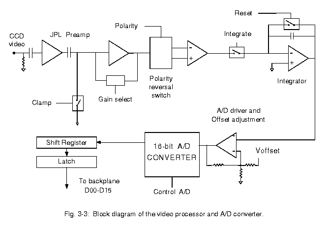
A classical resettable integrator is implemented by placing a capacitor in the feedback of U36, and placing the analog switch U32b across it. A similar switch U32a is placed in the signal path to disable integration when the signal is not valid. It is implemented as a dual slope integrator whereby the polarity of the amplifier U28 is selected to integrate up on the baseline after the CCD output node is reset but before charge is clocked onto it, and then to integrate back down after charge has been clocked onto the output node. The integrator reset switch is kept in the reset position whenever possible - during parallel clocking, command processing and image acquisition. The output of the integrator feeds the driver/offset op amp U42 that supplies a low impedance signal to the A/D converter. It is also connected through a voltage divider to one of the DAC outputs so a programmable output offset adjustment can be applied to the signal so zero detected charge on the CCD corresponds to a small number of A/D units, a particularly important consideration with the low capacitance/large feethrough CCDs that are now common. Additional inputs to the voltage divider are provided by R97 and R98 to allow the control of the zero point of the offset adjustment circuit, while R88 allows tailoring of the gain of the circuit so a sufficiently wide range is obtained. Each DAC count will change the A/D by approximately 217 counts in the default system. Larger values of R88 can be chosen to restrict the adjustment range while providing more resolution.
The overall gain of the video processor is set by several factors. The resistor ratio R26 and R28 in the non-inverting amplifier U4 set the gain of the preamplifier, and are set to a default value of x10. Similarly, the resistor pairs R46/R47 and R49/R50 set the gain of the next stage, providing default gains of x2 and x4. The integrator is set to provide unity gain with an 8 microsec integration time, and is normally operated close to unity gain, although there is a significant trade-off between integration time and readout noise. Overall, the video processor operates at a gain of 20 or 40. The A/D provides a maximum count output at an input voltage of 5.2 volts, from which it can be easily calculated that the sensitivity of the video processor is 4.0 and 2.0 microvolts per ADU for the low and high gain settings respectively. Operating CCDs with a node sensitivity near unity will result in overall system conversion constants close to these values, as measured in units of electrons per ADU.
Some users have reported innacurate signal handling performance with Tektronix CCDs. This seems to be related to the larger pedestal (difference between bias and signal levels) of the Tektronix CCDs compared to Loral CCDs, which causes overshoot or undershoot as bright stars are processed. This effect seems to be introduced by the output driving stage U42 becoming non-linear as it tries to recover from saturation. A workaround is to disconnect the capacitor C84 that filters the DAC offset voltage to the output amplifier. This will fix the problem, although a slight amount of noise is introduced - the video processor noise with a grounded input increased from 0.98 to 1.24 ADU in our tests. This is probably an insignificant noise source compared to CCD noise since they add quadratically, but users should be mindful of it. A better fix is being developed.
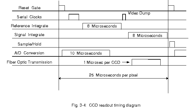
A 16-bit successive approximation analog-to-digital converter is implemented in U48 as a Crystal Semi- conductor monolithic CMOS part. A low noise and stable reference supply is implemented by U47 such that the difference between it and the incoming signal on AIN2 is converted to a ones complement number. The conversion is timed by an 8 MHz clock generated by the timing board by dividing down its 40 MHz clock, and serial output data is sent synchronously with this clock to two serial shift registers with latches (U62 and U64) for conversion back to a parallel format for transfer over the backplane. A timing signal (VP7) clocks data from the shift register to the internal latch of U62 and U64 so that the next pixel's data can be converted by the A/D before the current pixel data is read by the timing board. A reset input (VP0) is set low to put the A/D converter in a full recalibration cycle for 1.4 seconds to keep it within specifications. An approximate timing diagram of these video processor signals is shown in Fig. 3-4, with their relation to the serial clock waveforms and serial data transmission to the host computer.
A total of nine digital timing and setting control lines are needed to operate the video processor and A/D converter. Eight of these are generated by the latch U32 on the timing board, which updates all eight signals VP 0-7 simultaneously when the latch is written to. The ninth is needed by the video processor to set the gain of the DC restore, and is selected by setting the LATCH0 line to either a 0 (low gain) or a 1 (high gain). A summary of the nine control lines follows:
| Name | Function | Sense of control line |
|---|---|---|
| VP0 | Reset A/D | 0 to reset |
| VP1 | Coarse/Fine* select on A/D | 1 to start coarse sample |
| VP2 | Hold* on A/D | 0 to start A/D conversion |
| VP3 | Reset integrator capacitor | 0 to reset capacitor |
| VP4 | Integrate signal on integrator | 0 to integrate |
| VP5 | Polarity of dual slope integrator | 0 for baseline integration |
| VP6 | DC restore | 0 to DC restore |
| VP7 | Latch A/D counts | rising edge to latch data |
| LATCH0 | Select gain | 1 for high gain |
 Back to Document List Page.