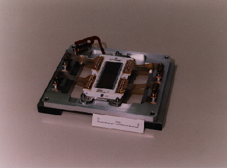

The University of Leicester in conjunction with EEV Ltd, began a development program in 1988 to produce large area, radiation hard CCDs with Fano limited energy resolution for the JET-X program. The starting point for this work was the commercially available P8600 device, originally designed as a CCD frame transfer array for 625-line TV applications. The end product is the P88903T (6) which is a large area (20.7 mm x 27.6 mm), multi-pixel (768 x 1024) three-phase front-illuminated MOS device. Its characteristics are summarised in Table 1. The response has been optimised across the soft X-ray energy range by incorporating several innovations into the design, in terms of materials, electrode structure and supplementary buried channel technologies. In order to obtain a reasonably high detection efficiency above a few keV, the CCDs are fabricated on high resistivity 1500 ohm-cm epitaxial silicon, 65 micron thick, on a 550 micron thick p+ substrate. For the nominal operating bias voltages, the devices are fully depleted to a depth of approximately 38 micron with a corresponding 27 micron field-free layer. The electrode structure has been thinned and narrowed to reduce the low energy cut-off due to the overlying electrode structure to 0.3 keV (defined to be the 5% quantum efficiency level). Specifically, the largest of the three electrodes (P3) which covers ~ 40% of the pixel area, is grown to a thickness of only 1700 Ĺ instead of the more usual 4000 Ĺ. Additionally, the protective oxide layer that normally covers P3 is also etched away to a residual thickness of 100 Ĺ.
        Table 1. Characteristics of the JET-X CCDs

CCD Parameter	Value

Pixel format on chip	    		    1024 x 768
Image format per pixel (pixels)		    512 x 768
Pixel size				    27 x 27 microns
Total active depth (epi-layer)		    65 microns
Depletion depth				    38 microns
Output node gain			    ~ 4 mV/ electron
Readout noise				    < 4 electrons rms
Readout rate per pixel			    12 microsec
Dark current @ -80 deg.C		    0.004/pixel/sec
Image frame time			    2.5 sec
Operating Temperature (start-of-life)	    180 - 190 K
Serial Charge Transfer Inefficiency	    < 1 x 10⁻⁵ per pixel
Parallel Charge Transfer Inefficiency 	    < 1 x 10⁻⁵ per pixel
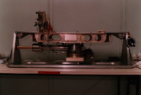
The JET-X focal plane optical bench containing the CCD cryostat

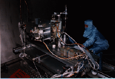
CCD calibration at MPE's Panter facility in Munich

Reference: A. Owens, A. Abbey, W. Burkert, H. Brauninger, C. Castelli, H. Chapman, J. Dowson, G. Fraser, Y. Li, K. McCarthy, P. Poole, M. Sims, J. Spragg, D. Watson, A. Wells and R. Willingale, submitted to J. X-ray Tech.